Hi everyone,
Servo: personally I´m not afraid of using a servo (if implemented right)
and we could get rid of the 1000 uF electrolytic cap in the
feedback loop this way. On the other hand I´m not afraid of
coupling caps either (as long as they are quality polypropylenes)
and the reason why I won´t probably not use a servo is simply
space resistrictions. I will have to stick with the original
module dimensions for fitting it into my ML-1.
(If you built a preamp from scratch you won´t have this limitations
of course.)
Maybe I could implement a servo on the RIAA network board later (and
try it with and without servo this way and see what it does soundwise,
probably HCK is right and it sounds better without it, I have not done
such a comparison yet)
What I´m thinking about is to add a capitance multiplier direct
on the modules (at least for the voltage gain stages) to address
the assymetric crosstalk issue (if space limitations permit it...)
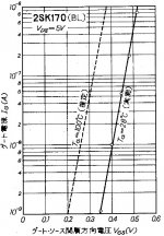
Simulation: You have 15.33mA through each input FET which is too
much for the components chosen. Using a matched quad of 2SK170V
would be an option. (most 2SK170V I have are around 14mA Idss).
I´ve read somewhere that John convinced the folks at Linear Systems
to make a higher Idss range than the V parts too, these would be
perfect here (once they are available).
0.55v before the source followers in HKC build:
Is this with the 1000 uF cap in the feedback loop (DC gain 1)
or without it ? It´s too much to be compensated with the offset
adjustment of the source followers I would say.
If you do not use the 1000 uF cap you will have a DC gain of
455 times, it will be hard to bring the offset down without a servo.
Hi gk7
I got the 0.55v with the 1000uF cap in the feedback network. I have been keeping the phono amp turned on for last 4 days and the offset is now lowered to 70~80mv.
Hi John
What is the ideal idss you would recommend for rest of the JFets in this circuit?
less than 15mA why is not recommend for?
when Idss is smaller we can increase Rd & decrease Rs,the way whether not good?
Sorry that I did not get back to answer questions, I didn't see this thread for awhile.
Unfortunately, I cannot give additional info on the JC-2 attenuators, as I did not design them.
The original JC-2 design was done in 1973, or 37 years ago. At that time, all we had available to us were Siliconix j-fets, in general, and for special applications, Union Carbide, Motorola, or Crystalonics.
The JC-2 phono input stage used Siliconix J110 input devices that are high current switches, that usually have an Idss of over 20 ma. The input devices were used at about 15 ma ea for lowest possible input noise. When you change the Id of the input devices in order to use lower Idss types, then you MUST change the load resistors, and this LOWERS the open loop bandwidth. Still, the change is not too great, IF you use high Idss devices like the 2SK170 V series. Running at 1/2 the originally designed current is not too different, BUT it will be another design if you run less.
The output j-fets of the phono stage. Lowering the Idss on these devices will lower the slew rate significantly, if taken too far.
The same problem with the complementary j-fets in the input driver stage. It is designed with a very high open loop bandwidth, on purpose, and this will be lost IF the input stage load resistors are increased too much. Still the V series 2SK170 and 2SJ74 series will work pretty well, for the output of the phono stage and the input of the line driver amp, with resistor changes.
Sorry that I did not get back to answer questions, I didn't see this thread for awhile.
Unfortunately, I cannot give additional info on the JC-2 attenuators, as I did not design them.
The original JC-2 design was done in 1973, or 37 years ago. At that time, all we had available to us were Siliconix j-fets, in general, and for special applications, Union Carbide, Motorola, or Crystalonics.
The JC-2 phono input stage used Siliconix J110 input devices that are high current switches, that usually have an Idss of over 20 ma. The input devices were used at about 15 ma ea for lowest possible input noise. When you change the Id of the input devices in order to use lower Idss types, then you MUST change the load resistors, and this LOWERS the open loop bandwidth. Still, the change is not too great, IF you use high Idss devices like the 2SK170 V series. Running at 1/2 the originally designed current is not too different, BUT it will be another design if you run less.
The output j-fets of the phono stage. Lowering the Idss on these devices will lower the slew rate significantly, if taken too far.
The same problem with the complementary j-fets in the input driver stage. It is designed with a very high open loop bandwidth, on purpose, and this will be lost IF the input stage load resistors are increased too much. Still the V series 2SK170 and 2SJ74 series will work pretty well, for the output of the phono stage and the input of the line driver amp, with resistor changes.
thank you very much
That´s very valuable information ideed, thank you very much. So I will use matched 2SK170V
for the input stage and adjust their drain resistors accordingly.
For the output stage the sad news is that more and more parts are unobtainable,
even Borbely Audio no longer has 2SK170V matched to 2SJ74V (all 2SK170V they
have left are 11.5-14 mA and all 2SJ74V 15-20 mA). Seems I have bought some
of the last matched quads when I built the line stage.
Maybe using BL grade and increase the number of pairs from 2 to 4 could be
an option. Or which other FETs for the output stage would be usable ?
That´s very valuable information ideed, thank you very much. So I will use matched 2SK170V
for the input stage and adjust their drain resistors accordingly.
For the output stage the sad news is that more and more parts are unobtainable,
even Borbely Audio no longer has 2SK170V matched to 2SJ74V (all 2SK170V they
have left are 11.5-14 mA and all 2SJ74V 15-20 mA). Seems I have bought some
of the last matched quads when I built the line stage.
Maybe using BL grade and increase the number of pairs from 2 to 4 could be
an option. Or which other FETs for the output stage would be usable ?
2N5434 Idss=30ma Vp=-1~-4v Ciss=30p Crss=15p
Doubling up is a reasonable solution for output devices, but resistance scaling is with a single pair of devices is better for input, because of the problem of higher nonlinear input capacitance.
Hi John
Could the input capacitance be minimized if each of the parallelled JFets connected with a source resistor?
If you want to reduce the input capacitance you could cascode them. In general I think you should not have problems with capitance modulation as long your source impedance is below 50 kOhms or so.
Hi gk7
Thank you for the inputs, cascode will change the structure of the circuit and that is not what I want to do. So I will leave it as the original as you said as long as the source impedance is below 50K Ohm.
- Home
- Source & Line
- Analog Line Level
- Need to build JC 2 preamp