"classic" amp and begginners problems (pcb wiring, component values)
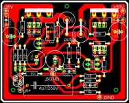
hi
i want to build this amp (based on esp design). My problems are:
1. The 10R resistor between SGND and GND is ok? or i do not have to put it there? if it is ok what power the resistor should be?
2. The capacitor groups (100n + 1000uF polarized, down left and down right corner), are a good choice?
3. Are the pcb traces wired correctly??? (i am not used to do pcb's and it's one of my fist tries)
4. I choose the BD139/140 + TIP35C/36C transistors, is this a good choice?
5. The output wires connect to the output pin for signal but i don't know if the output ground should be connected to the GND (power ground) or the SGND (signal ground, the star grounding point)
Please help me to get this right. I am new to amps. Thanks.
sorry the picture of the pcb didn't load up
An externally hosted image should be here but it was not working when we last tested it.
hi adi81bv,
A very good first attempt. I'm no expert but here is a few comments anyway.
1. The ground lift s OK. Some people use them, some don't, others put a diode or 2 across it.
2. I would prefer to see the filter caps closer to the output transistors. Check the diameter of the 1,000uF cap they seems to be small on the PCB. BTW: Rod reckons those caps are unecessary.
3. The accuracy of your traces really depends on your schematic. If you did the schematic right, and back and forward annotation is working then everything should be OK.
4. I haven't tried TIP35C/36C.
5. I'd put the output ground to the off board star earth.
With your power traces I'd try to have thick traces from the fuses to the filter caps then to the output transistors. Then take a thinner trace back to earlier stages.
With such a big board, the bottom right hand corner seems a little too cramped.
regards
A very good first attempt.
I'm no expert but here is a few comments anyway.1. The ground lift s OK. Some people use them, some don't, others put a diode or 2 across it.
2. I would prefer to see the filter caps closer to the output transistors. Check the diameter of the 1,000uF cap they seems to be small on the PCB. BTW: Rod reckons those caps are unecessary.
3. The accuracy of your traces really depends on your schematic. If you did the schematic right, and back and forward annotation is working then everything should be OK.
4. I haven't tried TIP35C/36C.
5. I'd put the output ground to the off board star earth.
With your power traces I'd try to have thick traces from the fuses to the filter caps then to the output transistors. Then take a thinner trace back to earlier stages.
With such a big board, the bottom right hand corner seems a little too cramped.
regards
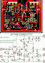
thanks greq
is it better now?
is it better now?
An externally hosted image should be here but it was not working when we last tested it.
Hi,
the Zobel must not link to the signal ground (SGND).
Take it to the power ground (GND) or it's own separate wire to offboard audio ground.
Change the shape of the output traces.
Connect the two emitter resistors with a straight wide trace.
Tap off this wide trace with a leg to feed the output pin and from the output pin a trace to the feedback pad.
From the trace feeding the output pin take off the Zobel link and the bootstrap link.
The speaker return and the PSU 0v and the Zobel return and the disconnecting network to safety earth and the signal ground and the power ground all meet at the off board audio ground.
Add an extra pin location on the input DC blocking cap to allow a better metallised film to replace the electrolytic.
Add two inverse parallel diodes (or zeners) across the NFB blocking cap.
Keep the big decoupling caps and KEEP the fuses.
Add two emitter degenerating resistors to the LTP pair (even if you decide to link them out).
ok i will put also the decoupling caps on the board
observation: for the people out there who ask themselves why I do not buy esp pcb. for me to buy a esp pcb is to expensive - due to custom fees and taking in account that i have no income and the components value for this amp is around only 2,5euro - so i think that building this pcb is no harm to rod. beside his pcb i understand is different from the schematics that he has on his site. hope you understand.
observation: for the people out there who ask themselves why I do not buy esp pcb. for me to buy a esp pcb is to expensive - due to custom fees and taking in account that i have no income and the components value for this amp is around only 2,5euro - so i think that building this pcb is no harm to rod. beside his pcb i understand is different from the schematics that he has on his site. hope you understand.
i am totally confused
1. do you have a link to some pictures how to make a star ground point?
here how i understand: i have 2 kinds of ground (GND and SGND) I collect the SGND on the PCB with a star and take a wire from this poit to a certain star point in the amp box. at this certain point i also collect the GND wires from PSU (0V or also known as reference voltage), ground (or return) from the speakers, GND from the amp pcb, GND from the preamp, box ground. Probably I mistake a lot.
-can anyone explain it to me( but in simple word, because i do not understand a lot of abbr. and terms.)
2. emitter degenerating resistors to the LTP pair - again can someone point me to a picture of an schematic - i presume that the LTP pair is Q1-Q2 transistors (BC546). From what i found these resistors are linked between GND and Q1-Q2 emitter?
3. in p3a schematic C3 100uF electrolytic cap is the NFB blocking cap. i received some info to add two inverse parallel diodes or zener across this cap. is this recommended? what value are the diodes? 1n4148 are ok? the diodes are inverse relative to them or the cap?
4. i modified the pcb again.... do you think this is better?
Attachments
Hi,
http://users.ece.gatech.edu/~mleach/lowtim/instage.html
shows the degeneration resistors on the emitters.
Read the whole site. You'll learn a lot about design.
You are getting tight for room.
Fit the degen resistors before NFB cap inverse // diodes.
yes, 1n4148 are OK but since they only hold 0.7v you need a series pair in each direction for 1.4v This allows a maximum of 1Vac across the cap before they bypass. But, that is now space for 4 diodes.
You need a signal ground next to the input at the cap.
Are you going to fit pads for an input electrolytic?
Are you going to move that Zobel off the signal ground?
I prefer your laid flat emitter resistors. Is there enough room?
-i will read the info there, thanks.
-i will not use an electrolytic cap for input, just the MKP( i already bought it today)
-there is no wary about puting emitter resistors like that (i tried this on other circuits and it is stable enough)
other questions:
-zobel will go directly to the star ground point or onto the GND on the pcb?
-so the degeneration resistors are placed near the LTP pair after the emitter. but what value and power this resistors are? (330R 1/2W?)
-can someone recommend a diode that has will hold 1,4V (is this what is necessary? can also be zener)
-what did you mean by this "Fit the degen resistors before NFB cap inverse // diodes."
you choose, but a separate wire to offboard ground looks less tidy.adi81bv said:zobel will go directly to the star ground point or onto the GND on the pcb?.........what value and power this resistors are? (330R 1/2W?).........can someone recommend a diode that has will hold 1,4V (is this what is necessary? can also be zener)..............what did you mean by this "Fit the degen resistors before NFB cap inverse // diodes."
>=125mW and between 22r and 330r.
Zeners are OK.
the Zeners are less important than the degeneration resistors.
Hi adi81bv.
On the schematic.
Have you run Tools > ERC?
You have extra junctions and some missing ones. If you use the Net command to place wires, the junctions are placed automatically. Use View > Show to check connectivity of nets. I often move components around to see the rubberbanding of the wires to confirm connectivity.
The schematic looks right.
On the PCB.
Have you run Tools > DRC > Check?
Red traces "normally" means the the traces are on the top of the PCB. On single sided PCBs, the traces are normally on the bottom and by default Eagle usually does these blue. Use the Change > Layer command to move them to the bottom.
Some of the traces seem very close to the pads. DRC should pick these up. Traces are usually done at 0, 45, 90, 135 angles only(for appearance).
regards
the schematic:
-yes i have extra joints - my mistake, about the missing ones, i do not see any.
the pcb:
-i use red because i am forced this way (by my printer who can print just red because its broken)
-about the pads, I'll check them before printing with laser for thermal transfer.
-i will put all the traces 45 degree multiple for best looks, but i have to be certain about the values of the components
So:
-The resistor between the SGND and GND i 'll use 10R/1W
-the SGND will be a star on the amp pcb, then a wire will go from the GND, SGND and zobel directly to the ground star point where will meet with the PE, 0V from PSU, box gnd, GND from vu-meter, and gnd from preamp.
-decoupling caps will be 100u/50V
-input caps i understand that 4u7/250V poli is a better choice
-the transistors i will put the on the heat sink with wires to the board
-100n caps i will use ceramic rated 50V.
hope i am correct
- Status
- This old topic is closed. If you want to reopen this topic, contact a moderator using the "Report Post" button.
- Home
- Amplifiers
- Solid State
- "classic" amp and begginners problems (pcb wiring, component values)