Pin orders in asy must be the same as model, this Pentode3.asy or use Pentode.asy and change pin order in model, either way will be ok.
Thanks. Opens fine now but same problem.
-222.76KV on the grids. 998.93mA on K1 and K2. R6 and R8 are carrying 1A each. How can a circuit with 500V in develop KV?
Attachments
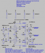
Open Pentode3.asy check the pin order matched or not in 6550a.inc
.SUBCKT 6550A A G2 G1 K ; 1 2 3 4
A=1, G2=2, G1=3, K=4
I use this 6550a.inc:-
.SUBCKT 6550A A G2 G1 K ; 1 2 3 4
A=1, G2=2, G1=3, K=4
I use this 6550a.inc:-
Code:
*
* Generic pentode model: 6550A
* Copyright 2003--2008 by Ayumi Nakabayashi, All rights reserved.
* Version 3.10, Generated on Sat Mar  8 22:42:21 2008
*             Plate
*             | Screen Grid
*             | | Control Grid
*             | | | Cathode
*             | | | |
.SUBCKT 6550A A G2 G1 K
BGG   GG   0 V=V(G1,K)+0.1919366
BM1   M1   0 V=(0.064698506*(URAMP(V(G2,K))+1e-10))**-0.90961742
BM2   M2   0 V=(0.62250546*(URAMP(V(GG)+URAMP(V(G2,K))/5.8346717)))**2.4096174
BP    P    0 V=0.0027588474*(URAMP(V(GG)+URAMP(V(G2,K))/9.3728844))**1.5
BIK   IK   0 V=U(V(GG))*V(P)+(1-U(V(GG)))*0.0017503674*V(M1)*V(M2)
BIG   IG   0 V=0.0013794237*URAMP(V(G1,K))**1.5*(URAMP(V(G1,K))/(URAMP(V(A,K))+URAMP(V(G1,K)))*1.2+0.4)
BIK2  IK2  0 V=V(IK,IG)*(1-0.4*(EXP(-URAMP(V(A,K))/URAMP(V(G2,K))*15)-EXP(-15)))
BIG2T IG2T 0 V=V(IK2)*(0.928052868*(1-URAMP(V(A,K))/(URAMP(V(A,K))+10))**1.5+0.071947132)
BIK3  IK3  0 V=V(IK2)*(URAMP(V(A,K))+2900)/(URAMP(V(G2,K))+2900)
BIK4  IK4  0 V=V(IK3)-URAMP(V(IK3)-(0.0018325138*(URAMP(V(A,K))+URAMP(URAMP(V(G2,K))-URAMP(V(A,K))))**1.5))
BIP   IP   0 V=URAMP(V(IK4,IG2T)-URAMP(V(IK4,IG2T)-(0.0018325138*URAMP(V(A,K))**1.5)))
BIAK  A    K I=V(IP)+1e-10*V(A,K)
BIG2  G2   K I=URAMP(V(IK4,IP))
BIGK  G1   K I=V(IG)
* CAPS
CGA   G1  A  0.8p
CGK   G1  K  8.6p
C12   G1  G2 5.7p
CAK   A   K  9.2p
.ENDSI use this 6550a.inc:-
Same as mine:
6550A.inc: .SUBCKT 6550A A G2 G1 K
pentode3.asy:
PINATTR PinName Anode
PINATTR SpiceOrder 1
PIN -48 0 NONE 0
PINATTR PinName G1
PINATTR SpiceOrder 3
PIN 32 48 NONE 0
PINATTR PinName Cathode
PINATTR SpiceOrder 4
PIN 48 -16 NONE 0
PINATTR PinName G2
PINATTR SpiceOrder 2
@45
<snip> Meanwhile, I've applied what I've learned here to modelling the Van der Veen 4070-CFB-PP transformer.
Before arithmetic comes the logic of comparison. So if you want to see the effect of cathode feedback and you want to use the Polish 4K transformer with CFb then you can't optmize for 4K without CBf and assume that it will be fine with CFb on! So when you run the simulation without CBf you have to use ANOTHER transformer that has got all those cathode winding turns at the plate so that the primary load is 7K. Otherwise you are comparing two amplifiers where very likely one is optimised in the way you want (for example max power with minimum distortion) and the other won't be! Instead if you compare 7K standard transformer with 4K+24% CBf the operative conditions of the output stage stay the same. The point is that 24% CFb is a lot.
With the VDV, especially the 4070, you can skip this passage because the difference between CFb and non-CFb is much smaller being the CBf 5-10% only. So the compromise is much smaller or even negligible for practical purposes.
...Looks like I need less CFB....
Or more driver.
Remember Macintosh managed 50% cathode FB, albeit with a super-strapped (or transformer!) driver.
Open both files in LTSpice, check to make sure it has loaded the correct files. If still don't work change to another LTSpice version or reboot you computer.
Thanks. I have this working now.
I changed the 6550A include to point to my Ayumi library. The file there looked the same as the copy I had in the sim folder so I don't know what the problem was. Didn't work before I changed the include but worked after.
Not only do I now have a useful transformer test sim but I've learned a couple of tricks as well. I like how you use net names, resistors and capacitors to provide off-model test points. I'll do that in my sims.
Is there any way I can use the sim to calculate the effective primary impedance?
The constant current (just type "cur" in LTSpice will locate it) is used to connect to any input/output to measure the impedance. If there is DC, a capacitor is used to block it. Since only the primary Z is measured, the speaker load 4/8 ohms should disconnected or connected for overall result. You can disable the load also by excluding it from the coupling factor K.
Z=V/I, I being current drawn in current source, to plot this add these 2 traces and set limits to linear.
I hope this makes sense.
Z=V/I, I being current drawn in current source, to plot this add these 2 traces and set limits to linear.
I hope this makes sense.
Attachments
Last edited:
Thanks very much for this. More I've learned!
However, I am unable to plot impedance. Expression is correct but still showing level and phase. I must have missed something.
Referring to your plot, it appears that Z decreases as Lcfb increases. Is that correct?
However, I am unable to plot impedance. Expression is correct but still showing level and phase. I must have missed something.
Referring to your plot, it appears that Z decreases as Lcfb increases. Is that correct?
Attachments
Yes, as Lcfb increased, Nfb increased so the Ra decreased. You can insert the current source in between P-1 and P-2 to get full Ra-a. In this case there is no voltage difference between P-1 and P-2 so the block cap is not needed and gives you more accurate result.
To display impedance level in ohms, on the waveform window, right click to bring up popup manual, click on the "Manual Limits", on "Left Vertical Axis", select "Linear"
To turn off the phase plot, left click on right axis (phase) to bring up popup manual, click on "Don't Plot Phase".
To display impedance level in ohms, on the waveform window, right click to bring up popup manual, click on the "Manual Limits", on "Left Vertical Axis", select "Linear"
To turn off the phase plot, left click on right axis (phase) to bring up popup manual, click on "Don't Plot Phase".
Attachments
Last edited:
Got it. Thanks again! That is really clever. I even worked out how to add the labels.
Plot of full Ra-a attached.
Earlier you said "Since only the primary Z is measured, the speaker load 4/8 ohms should disconnected or connected for overall result."
I thought the primary Z is supposed to be 4K (in this case) WITH the 8Ω load attached. I see you have R2 set to 80K. I'm obviously misunderstanding something here.
Thanks. I had to read this a few times but it makes good sense.
Yes, as Lcfb increased, Nfb increased so the Ra decreased. You can insert the current source in between P-1 and P-2 to get full Ra-a. In this case there is no voltage difference between P-1 and P-2 so the block cap is not needed and gives you more accurate result.
Plot of full Ra-a attached.
Earlier you said "Since only the primary Z is measured, the speaker load 4/8 ohms should disconnected or connected for overall result."
I thought the primary Z is supposed to be 4K (in this case) WITH the 8Ω load attached. I see you have R2 set to 80K. I'm obviously misunderstanding something here.
So if you want to see the effect of cathode feedback and you want to use the Polish 4K transformer with CFb then you can't optmize for 4K without CBf and assume that it will be fine with CFb on! So when you run the simulation without CBf you have to use ANOTHER transformer that has got all those cathode winding turns at the plate so that the primary load is 7K. Otherwise you are comparing two amplifiers where very likely one is optimised in the way you want (for example max power with minimum distortion) and the other won't be! Instead if you compare 7K standard transformer with 4K+24% CBf the operative conditions of the output stage stay the same. The point is that 24% CFb is a lot.
Thanks. I had to read this a few times but it makes good sense.
Attachments
Plot of full Ra-a attached.
Earlier you said "Since only the primary Z is measured, the speaker load 4/8 ohms should disconnected or connected for overall result."
I thought the primary Z is supposed to be 4K (in this case) WITH the 8Ω load attached. I see you have R2 set to 80K. I'm obviously misunderstanding something here.
If the load is connected you can see overall result which the is result of both current source and load in parallel. So to measure the output impedance of secondary the load is also set to very high or disconnected.
If connected it's the overall result of both in parallel (sorry for not clarify earlier).
But the thing is that the secondary output Z measured is about 16 Ohms instead of 8, with 0H Lcfb, what gives?
PS: So if we connect 16 Ohms to secondary, and then pri Z measured again between P-1 and P-2 is 2k (half of 4k measured earlier), that is result in parallel of current source and (reflected) load.
Attachments
Last edited:
If the load is connected you can see overall result which the is result of both current source and load in parallel. So to measure the output impedance of secondary the load is also set to very high or disconnected.
If connected it's the overall result of both in parallel (sorry for not clarify earlier).
But the thing is that the secondary output Z measured is about 16 Ohms instead of 8, with 0H Lcfb, what gives?
Ahh. It makes sense now.
But the thing is that the secondary output Z measured is about 16 Ohms instead of 8, with 0H Lcfb, what gives?
What indeed! I hope you're not asking me! I'll be interested to know the answer to that.
So, you could also plot damping factor.
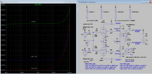
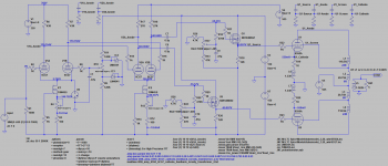
Simulation with the VDV4070CFB Transformer
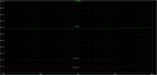
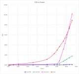
Schematic is shown in the first attachment. THD vs Power is shown in the second attachment.
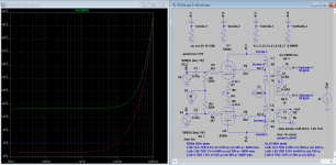
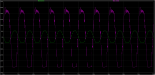
THD at 50W is estimated as 3%. The MOSFET screen and output anode traces in the third attachment look pretty awful!
koonw’s output stage simulation suggests 0.5% THD at 50W. Maybe this is a result of the perfect signal sources in that simulation.
THD at the MOSFET sources deteriorates rapidly after 50W output due to clipping of the negative cycles (3rd attachment). I can fix that by changing the MOSFET negative supply from -150V to -200V but that doesn't have much impact on the output stage because the 6550s are turned off then anyway.
Menno van der Veen reports 50W for this configuration but doesn’t give any THD data.
Any suggestions how I can improve the performance of the sim or the circuit?
Schematic is shown in the first attachment. THD vs Power is shown in the second attachment.
THD at 50W is estimated as 3%. The MOSFET screen and output anode traces in the third attachment look pretty awful!
koonw’s output stage simulation suggests 0.5% THD at 50W. Maybe this is a result of the perfect signal sources in that simulation.
THD at the MOSFET sources deteriorates rapidly after 50W output due to clipping of the negative cycles (3rd attachment). I can fix that by changing the MOSFET negative supply from -150V to -200V but that doesn't have much impact on the output stage because the 6550s are turned off then anyway.
Menno van der Veen reports 50W for this configuration but doesn’t give any THD data.
Any suggestions how I can improve the performance of the sim or the circuit?
Attachments
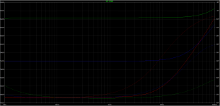
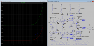
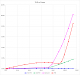
Leakage inductance
Thanks. That made a huge difference! THD < 1.2% up to 80W. the simulation even shows it dropping to 0.9% at 90W. Output tube dissipation at that point is still only 25W.
I'll read up on modelling the leakage inductance. I've read that toroidal transformers have lower leakage inductance than traditional EI cores. I'll also do deeper into Norman Koren's The Emperor's New Amplifier.
Attachments
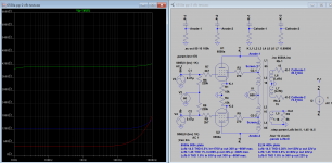
THD at the MOSFET sources deteriorates rapidly after 50W output due to clipping of the negative cycles (3rd attachment).
Before you changing anything, look at output tube G1 waveform in the simulator.
About +30V.... -150V swing.
Then look in 6550 datasheet the UL characteristic: 0V... -70V swing.
No comment.
- Status
- This old topic is closed. If you want to reopen this topic, contact a moderator using the "Report Post" button.
- Home
- Design & Build
- Software Tools
- LTSpice model for a commercial toroidal output transformer