Help with Kicad
Hi I am making a PCB for my new amp using Kicad. But I think my Gerber files look weird compared to the videos I can find on YouTube. Can some one tell me, if the numbers on the on the layout will mess up the fabrication, or how to remove them.
Thanks in advance
Hi I am making a PCB for my new amp using Kicad. But I think my Gerber files look weird compared to the videos I can find on YouTube. Can some one tell me, if the numbers on the on the layout will mess up the fabrication, or how to remove them.
Thanks in advance
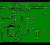
Attachments
Depends on the board fab. The fabs I use, seem to automatically delete graphical lines on the FrontSilkScreen (and BackSilkScreen) layers, which overlap the SolderMask layers.
You could use GerbView to display only the soldermask layers and the silkscreen layers, to get a rough idea of how much text the fab may delete.
I don't know how the text got there in the first place, so I don't know how to make it disappear. You may need to start Googling for "KiCad unwanted node text" and other such descriptions.
Those are D-codes. I think they're in all Gerber files. Just go to Preferences in GerbView and uncheck "Show D codes".
Thanks Jeff
Gerber is actually a photo plotter format and the D codes are referencing different holes sizes in a mask, for exposing the photo sensitive resist or even photographic film in the old days. They won't appear on your PCB.
Thanks for the info. I guess a good day is a day where you learn something new
")
- Status
- This old topic is closed. If you want to reopen this topic, contact a moderator using the "Report Post" button.
- Home
- Design & Build
- Software Tools
- Help with Kicad