Thats pretty standard, it gives you nice short connections down from the top to the plane, and a solid plane is a good thing (which you will not have if you put it on top because of the components).
My default 4 layer stackup is Routing, Gnd, Power, Routing, makes probing nets during development easier apart from anything else, buried routing is a pain when you need to roach wire something).
Regards, Dan.
My default 4 layer stackup is Routing, Gnd, Power, Routing, makes probing nets during development easier apart from anything else, buried routing is a pain when you need to roach wire something).
Regards, Dan.
looking around the net it mostly says to have the ground plain on layer 2 rather than the top, is this correct?
That depends entirely on what you want to achieve. If you need impedance controlled traces, you'll likely need those on top with a ground on the second layer. For analog layouts, you'd need to look at the impedances to the various planes and layers and make a decision as to where to optimize. There's no universal answer.
Tom
I concur, there are thousands of 4 layer designs that follow the above stack up, we use that as standard for any 4 layer board.
The advantage of the 0V plane on layer two is you can reduce the slots caused by through holes (suppress inner layer pads, but add 0.15mm drill oversize, or reduce inner layer pads to 0.15mm (0.006") over the drill size.) and where SMD is used you get an almost contiguous plane.
Er sorry for quick OT but Mr Mills are you responsible for this little Teez er
Dry, Marce, very dry, but not wrong.
There are a lot of ways to arrange a 4 layer stackup. Having ground on an inner layer means that all grounds go through a via. This adds a tiny bit of inductance, but more importantly, unless you're using expensive blind vias, you're putting a hole through the entire stackup, which takes up a lot of space if you're using cheap, wide vias (15 mil drill). These large holes and their even larger keepaway radius can almost always be avoided with ground on top and bottom.
I use SMD almost exclusively, so I use the outer layers for routing, and lay out ground using a copper pour. This means that I don't get a huge uninterrupted ground, but if the components are spaced and arranged nicely, there's plenty of well connected foil to provide a very substantial, low impedance ground. I use the inner layers for power and additional routing as needed.
Again, as has been said before, there are many ways to approach a stackup, but I find that it's easier for me to minimize the number of vias/drills by placing most ground and routing on the outer layers. I don't need controlled impedance traces, but I still need a low impedance ground, and this seems to work pretty well for me. The resulting boards end up being pretty dense.
If you're primarily using through hole, then my scheme might not be ideal, - my goal of minimizing drills is probably silly unless you're using nearly 100% SMD. But, my main point is that it's not necessary to dedicate an entire layer to only one function. It's just copper spaced by some dielectric of different thicknesses, and you can do what you want with it.
For testing, I like having a quality ground foil next to the routing traces and components, and not buried inside of a stackup. This makes it much easier to connect a scope probe and be able to trust HF and low level signals - a good wideband probe ground is always a few mm away.
Best of luck!
A copper poured ground round routes and components is NOT a ground plane, a ground plane is a contiguous plane on a single layer with no slots (careful placement of vias...).
This ground plane (horrible name, it should be referred to as either 0V or return) will then provide an uninterrupted return path for the higher frequency signals. Any discontinuity in the return path causes noise:
Slots in Ground Planes
On any boar I do the ground plane is king and there shall be no tracks or slots, this is the one rule of PCB design that I never allow to be broken....
When doing two layer boards I try and keep the secondary side as clear as possible to create a ground pour, luckily these days very rarely do 2 layer boards the price difference for going to 4 makes it a viable proposition except for the most cost conscious designs... The majority of boards I do are usually 6-14 layers these days, with multiple ground planes and power pairs (voltage and a closely coupled ground plane to get some planar capacitance, dielectric >0.1mm)
Last edited:
If you can, make 1 layer completely filled with copper (inner layer, usually layer 2) and make this layer GND/COM. Section off highspeed circutry and analog circuitry placing the analog circuits as close to the output connectors as possible. Via GND as close as possible from top and bottom layer CAPs and IC GND pins.
Like Marce said, any breaks in the GND plane is bad news. Return currents start to fly everywhere. Anything Marce says is correct, he knows PCB layout!
Any 2 layer boards I do I try and make the bottom layer completely GND pour. Place all parts on Top and try as much as possible to route all signals and fat power lines on the top copper layer. 2 layer PCBs are tricky to do well.
Sorry for the snarky response, but a few things to keep in mind. The circuit I refer to is completely balanced, so there are no return currents 'flying around' that need to be bludgeoned with a perfect ground plane. Every connection to ground has a signal polarity inverted dual, and their currents are arranged to cancel over a small patch of foil. Further, I'm using a clever power supply scheme that prevents the rectified op amp supply currents from traveling throughout ground. Finally, while this circuit uses 100MHz op amps, there is no need for controlled impedance lines. It's clearly in 'lumped land', with no traces that need to be treated as transmission lines. Because of this, the penalty of an imperfect ground plane is a little less copper and a little higher impedance. Again, I do not care exactly what impedance ground or traces routed over ground are, I just need ground to be low impedance over a wide bandwidth.
You're welcome to do what you like, but it's not true that all PCBs without a 'perfect' ground plane are doomed to failure. I can't afford a 6 layer board, and I don't need it apparently either. Actually, the performance numbers I quoted above are for the single sided version - the 4 layer is still being assembled.
You're welcome to do what you like, but it's not true that all PCBs without a 'perfect' ground plane are doomed to failure. I can't afford a 6 layer board, and I don't need it apparently either. Actually, the performance numbers I quoted above are for the single sided version - the 4 layer is still being assembled.
Glad that you got it to work out Monte. My comment of "flying around" refers more towards mixed signal boards (please refer to previous post) but I didn't know an uninterrupted plane on a purely analog board did not have the potential to improve things .
.
I didn't mean to infer in my other posts that other techniques are doomed to failure or that a 2 layer board in this instance is not the way to go, simply that everything I have read of marces posts appear factually correct according to literature and matches my own experience in PCB design, nothing more. You could call be a marce fanboy! I'm welcome to be corrected on technical issues as it would make me a better designer but....
I believe it is a fair comment for best practices to encourage the use of unbroken ground plane when possible. It would be easier to get right when running I2S and MCLK lines going to your DAC on a 4 layer pcb with the instructed use of GND plane as I2S are not balanced lines drives. I prefer to avoid running analog traces under/over other analog traces if possible. As with everything there is always a compromise and one chooses their which ones to address.
I have no doubt there are many of you well versed in tricky layouts. Happy listening!
If you're tied to Eagle, it looks like $315 will get you the Standard Layout. That'll handle up to six layers. $575 will get you Schematic + Layout Standard. I do understand that $575 is a fair chunk of change, but is actually pretty low for a schematic + layout package. Have a look at the pricing for Altium or OrCAD for a realistic comparison.
Tom
You don't have to spend anything like that to get a decent PCBCAD package.
The high cost packages just have loads of stuff a hobbyist might never use.
A quick internet search brings up loads of free software and many of those do multiple layers.
i think i have finished, just need to make the gerbers.
i have put a 14mil pad/hole isolation on all boards.
Work Board:
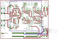
L1_Signal:
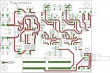
L2_GND:
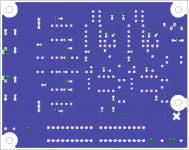
L3:V-:
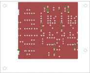
L4_V+, Signal:
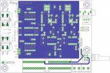
i had a play with Kicad to see what it done with 4 layer boards and it left the pads on all layers. what i have done is replaced the unused pads with holes which gives more real estate for copper pours.
drill/mill will be top layer for all layers.
i have put a 14mil pad/hole isolation on all boards.
Work Board:

L1_Signal:

L2_GND:

L3:V-:

L4_V+, Signal:

i had a play with Kicad to see what it done with 4 layer boards and it left the pads on all layers. what i have done is replaced the unused pads with holes which gives more real estate for copper pours.
drill/mill will be top layer for all layers.
Don't see as many 2 layer boards as I used to, but seen plenty in the past that have worked....
I am intrigued by your design Mr McGuire and would be interested in seeing it... Balanced signals and routing does minimise the effects of bad ground (as does LVDS for digital, hence its increasing popularity as the defacto interface, HDMI Ethernet, USB data transfer, some handshaking is single ended hence USB requires a ground connection). The beauty of balanced is the return currents will flow down the opposite leg of the balanced connection, though on a PCB you have to be careful how you route them when ground planes are present as the return can couple to this plane depending on the board stack up and dielectric distances. Pseudo balanced routing can also be used for sensitive analogue signals to again minimise the interaction with the full ground, do this quite often when bringing low level mic signals onto a board and to the first active device, often broadside routed to get good coupling between the hot and return, the ground connection is then done very near the input to the first active device. This is for single ended signals only.
Bibio don't totally remove pads on inner layers unless your software has a drill oversize function, if it doesn't leave a land that is 0.15mm (6 thou) larger than your required finished hole size (0.2mm/8 thou) if space allows this is to cater for the fact that PTH holes are drilled larger than your finished hole spec (approx. 0.1mm) and to allow for PCB fabrication tolerances...
Bibio don't totally remove pads on inner layers unless your software has a drill oversize function, if it doesn't leave a land that is 0.15mm (6 thou) larger than your required finished hole size (0.2mm/8 thou) if space allows this is to cater for the fact that PTH holes are drilled larger than your finished hole spec (approx. 0.1mm) and to allow for PCB fabrication tolerances...
ok. i was going by the drillfile sizes that includes the plating tolerances.
whats the minimum isolation on pours i can safely use?
The drill sizes you specify in your PCB file are finished hole sizes after processing and plating...
So if you specify a 1mm hole the manufacturer will use a 1.1mm drill to drill the unplated hole... You also have to allow for fabrication tolerances so don't remove inner layer pads just make them a bit larger than the finished hole size, adding 0.2mm would be sufficient, so your pad on an inner layer for a 1mm hole would be 1.2mm
So if you specify a 1mm hole the manufacturer will use a 1.1mm drill to drill the unplated hole... You also have to allow for fabrication tolerances so don't remove inner layer pads just make them a bit larger than the finished hole size, adding 0.2mm would be sufficient, so your pad on an inner layer for a 1mm hole would be 1.2mm
- Status
- This old topic is closed. If you want to reopen this topic, contact a moderator using the "Report Post" button.
- Home
- Design & Build
- Software Tools
- Sending files to PCB fabricators