Hello,
I just got myself a Cambridge Audio A500 amplifier and right now I'm looking at replacing all the electrolytic caps inside. It's '98 vintage, one bulged small capacitor from the output of a +30V regulator.
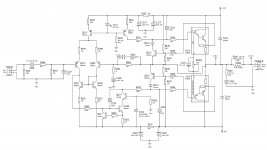
But I also want to sim the output stage. I am having trouble with the output transistors, SAP15 darlington types with diodes and emitter resistor included in the capsule.
Mooly recommended I use a VBE multiplier instead of the bias circuit with the diodes but I didn't have any luck so far. I can bias the emitter resistor from the NPN transistor. But the PNP stays at 2A or so.
I did manage to make the schematic work by adding all the diodes in the package schematic of SAP15, but I got some oscillation in the sim and I don't think that's the way to go here.
What am I doing wrong with the VBE multiplier?
I used the resistor values from the SAP15 datasheet. The diodes I just guessed and it worked.
I attached both versions.
I just got myself a Cambridge Audio A500 amplifier and right now I'm looking at replacing all the electrolytic caps inside. It's '98 vintage, one bulged small capacitor from the output of a +30V regulator.
But I also want to sim the output stage. I am having trouble with the output transistors, SAP15 darlington types with diodes and emitter resistor included in the capsule.
Mooly recommended I use a VBE multiplier instead of the bias circuit with the diodes but I didn't have any luck so far. I can bias the emitter resistor from the NPN transistor. But the PNP stays at 2A or so.
I did manage to make the schematic work by adding all the diodes in the package schematic of SAP15, but I got some oscillation in the sim and I don't think that's the way to go here.
What am I doing wrong with the VBE multiplier?
I used the resistor values from the SAP15 datasheet. The diodes I just guessed and it worked.
I attached both versions.
Attachments
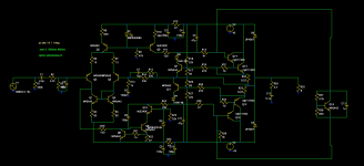
") The MJL's were intended just for the outputs, not the drivers as well.
The MJL's were intended just for the outputs, not the drivers as well.Oh, I understand now.
I never had to deal with Darlington transistors and I didn't have any idea on their structure. I presumed both transistors were the same.
And I see that you removed the protection transistors as well so you can correctly bias the output with the VBE multiplier.
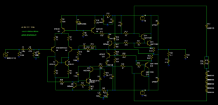
I did chase some numbers in Spice and with KSC1845/KSA992 and KSC2690/KSA1220 I managed to get a nice THD of 0.000679% at 1W into 8ohm.
But that is not what real life will give. As there are many factors that have to be taken into account. I see the bias current is twice the amps recommended and it's different output device etc. Lots of things to consider.
Thanks for the help Mooly, I will now play some more with the model so I understand the topology.
I never had to deal with Darlington transistors and I didn't have any idea on their structure. I presumed both transistors were the same.
And I see that you removed the protection transistors as well so you can correctly bias the output with the VBE multiplier.
I did chase some numbers in Spice and with KSC1845/KSA992 and KSC2690/KSA1220 I managed to get a nice THD of 0.000679% at 1W into 8ohm.
But that is not what real life will give. As there are many factors that have to be taken into account. I see the bias current is twice the amps recommended and it's different output device etc. Lots of things to consider.
Thanks for the help Mooly, I will now play some more with the model so I understand the topology.
Protection circuitry just complicates the diagram for a basic simulation. If the real distortion figure were ten or even a hundred times worse, it would still be pretty good. One problem with simulation is that transistor matching between the same devices is of course perfect because the models are identical. For a real worst case try different devices for each transistor. See what difference it makes.
- Status
- This old topic is closed. If you want to reopen this topic, contact a moderator using the "Report Post" button.