Hello guys,
I'm new to building my own pcbs so I would really appreciate if someone could please make a pcb layout from this schematic picture
I've tried for hours using PCB Creator and Eagle but I couldn't find a way to do to make the routes work, and please attach the schematic file as well as the pcb layout file so I could learn.
Thanks in advance.
Call it "tough love" if you'd like...
IMHO you're not trying hard enough, or you're over-thinking the problem. This PCB is about as easy as it gets. If need be, use jumper wires (ie 0Ω resistors) to cross over other traces that are in the way (assuming a single-sided board).
Is the difficulty in connecting pins 5 and 13, and/or pins 3, 7, & 11? The other connections are fairly straightforward.
PCB
You MIGHT try using google and looking for a PCB latout....
Hello guys,
I'm new to building my own pcbs so I would really appreciate if someone could please make a pcb layout from this schematic picture
I've tried for hours using PCB Creator and Eagle but I couldn't find a way to do to make the routes work, and please attach the schematic file as well as the pcb layout file so I could learn.
Thanks in advance.
You MIGHT try using google and looking for a PCB latout....
You MIGHT try using google and looking for a PCB latout....
Thanks for the reply,
well I tried google but couldn't find a layout for this exact schematic I found one that is similar with a few changes and I also want to understand how its made so a picture only from isn't enough
Call it "tough love" if you'd like...
IMHO you're not trying hard enough, or you're over-thinking the problem. This PCB is about as easy as it gets. If need be, use jumper wires (ie 0Ω resistors) to cross over other traces that are in the way (assuming a single-sided board).
Is the difficulty in connecting pins 5 and 13, and/or pins 3, 7, & 11? The other connections are fairly straightforward.
Okay thanks I'll try to do it like you said and sorry but I'm very new to this stuff and realy trying to learn also I wanted it as an example to learn from.
Last edited:
Call it "tough love" if you'd like...
IMHO you're not trying hard enough . . .
Yeah, seeding a search engine with "tda1554 pcb" seems to turn up several candidates.You MIGHT try using google and looking for a PCB latout....
On this Forum, and similar venues covering a WIDE range of subjects at both hobby and professional levels, basic etiquette requires participants seeking help to show that they have made some effort to find a solution to their problem. At a very fundamental level this separates the "gimme" from the "teach me" attitude. Those who have neither the time nor the inclination to adopt a "teach me" approach are sometimes advised to engage the services of a professional design engineer; an apprentice costs about $30/hr and up, while those with their feces amalgamated command double that rate or more.
If you have a PWB layout for a similar circuit but don't have access to PWB layout software you can still use something like Microsoft "Paint" to mark-up an image with the changes you think are necessary to meet your requirements. I'll bet that Forum members will let you know if the changes are electrically correct, and probably throw in gratis comments on trace routing, component placement, etc.
PWB layout is definitely an art. Your instinct suggests it can be learned by studying and replicating the works of master artisans and there is a great deal of truth to that. Innate ability, perseverance, opportunity, and confidence - as well as the previously mentioned competent instruction - all play a role, though these qualities can be traded off against each other to some degree.. . . . all good things—trout as well as eternal salvation—come by grace and grace comes by art and art does not come easy.
- Norman Maclean, from "A River Runs Through It"
Walking the path from minimal adequacy through mediocrity to mastery takes time and effort. That's the way the "perversity of nature" - or, as Maclean would probably call it, the "fallen creation" - works. Others walking the path sometimes leave blazes or guidelines along the trail, which are nearly meaningless until you happen to be passing that exact location, so don't be discouraged if some advice you encounter doesn't make sense. I daresay every professional master has, at some time, looked at a layout and asked "Who was suffering from a cranial-rectal inversion when they created this?" - only to find their own initials in the last block of the "Revisions" record.
Your circuit, while basic, has some subtle pitfalls. 40 watts (total) power is far from "high power" by most standards but it's a LOT more than you find in small-signal circuits. It's important to identify the high-current traces, adequately size them, and route them to avoid coupling from either electromagnetic effects or IR drops. There's also a large amount of potential gain floating around in this circuit. Each channel is only 26 dB (20 V/V) but accidental coupling from one channel to another could create a power oscillator. And don't be fooled by the idea that this chip amplifies "only" audio frequencies; I'll bet sections within that IC have bandwidths extending well into the MHz range.
I'm hardly competent to pass judgement, but I still look forward to seeing the results of your efforts! One of these days I'll do some chip amp project so we can learn together.
Dale
Yeah, seeding a search engine with "tda1554 pcb" seems to turn up several candidates.
On this Forum, and similar venues covering a WIDE range of subjects at both hobby and professional levels, basic etiquette requires participants seeking help to show that they have made some effort to find a solution to their problem. At a very fundamental level this separates the "gimme" from the "teach me" attitude. Those who have neither the time nor the inclination to adopt a "teach me" approach are sometimes advised to engage the services of a professional design engineer; an apprentice costs about $30/hr and up, while those with their feces amalgamated command double that rate or more.
If you have a PWB layout for a similar circuit but don't have access to PWB layout software you can still use something like Microsoft "Paint" to mark-up an image with the changes you think are necessary to meet your requirements. I'll bet that Forum members will let you know if the changes are electrically correct, and probably throw in gratis comments on trace routing, component placement, etc.
PWB layout is definitely an art. Your instinct suggests it can be learned by studying and replicating the works of master artisans and there is a great deal of truth to that. Innate ability, perseverance, opportunity, and confidence - as well as the previously mentioned competent instruction - all play a role, though these qualities can be traded off against each other to some degree.
Walking the path from minimal adequacy through mediocrity to mastery takes time and effort. That's the way the "perversity of nature" - or, as Maclean would probably call it, the "fallen creation" - works. Others walking the path sometimes leave blazes or guidelines along the trail, which are nearly meaningless until you happen to be passing that exact location, so don't be discouraged if some advice you encounter doesn't make sense. I daresay every professional master has, at some time, looked at a layout and asked "Who was suffering from a cranial-rectal inversion when they created this?" - only to find their own initials in the last block of the "Revisions" record.
Your circuit, while basic, has some subtle pitfalls. 40 watts (total) power is far from "high power" by most standards but it's a LOT more than you find in small-signal circuits. It's important to identify the high-current traces, adequately size them, and route them to avoid coupling from either electromagnetic effects or IR drops. There's also a large amount of potential gain floating around in this circuit. Each channel is only 26 dB (20 V/V) but accidental coupling from one channel to another could create a power oscillator. And don't be fooled by the idea that this chip amplifies "only" audio frequencies; I'll bet sections within that IC have bandwidths extending well into the MHz range.
I'm hardly competent to pass judgement, but I still look forward to seeing the results of your efforts! One of these days I'll do some chip amp project so we can learn together.
Dale
Thanks for your reply Dale,
there is some truth to what you said but not all of it is true I'm trying to learn and not following a "gimme" approach but since this is my very first circuit I just thought that I would need an example to get me started also my free time is very limited those days and I'm spending every minute on this project this circuit is a part of a 5.1 amp that I'm trying to make and believe me if I had the money I wouldn't build this myself I would have replaced the speakers altogether not because I don't like electronics but because the lack of time anyway I have gathered some more info and learned some new things and put everything I have into this pcb please take a look at it and tell me what you think
Attachments
It's simply my position that "do it for me, please" is counter to the foundation of this forum. But direction and guidance isn't below anyone. I'm not, regrettably, as skilled as I'd like to be with board layouts; I just did a chip amp board last weekend that I think is okay, but I want to go over it for a few days with fresh eyes before committing solder.Okay thanks I'll try to do it like you said and sorry but I'm very new to this stuff and realy trying to learn also I wanted it as an example to learn from.
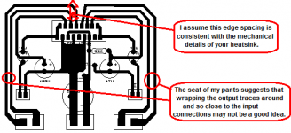
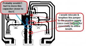
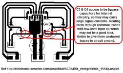
I said previously that most of the connections are straightforward; they mostly join to nearby pins. So the best course is to place them as near the chip as possible. The others, like pins 3 & 5, may possibly be joined to other pins right under the chip, with short traces. Perhaps the inputs and/or outputs don't need to run to the board edge, which could then leave some room to maneuver other traces.
Throughout the layout process, keep in mind the tracks that carry higher power, as mentioned. Keep inputs well separated from outputs. Have a grounding scheme in mind to minimize loop currents.
Give it another go and post your result.
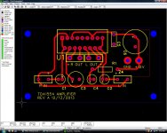
Not at all familiar with this chip but here are my thoughts.. . . please take a look at it and tell me what you think
Dale
Attachments
Not at all familiar with this chip but here are my thoughts.
Dale
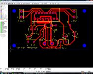
Thanks alot for giving me your opinion on the layout unfortunately I made and it did not work the speakers just made a low hissing noise with a messed up version of the music I was playing.
I think I'll need to find another schematic and start over

I googled and the second image found was....... wait for it.....
I would agree with the other members here, you made no effort but want to be spoon fed. Type TDA1554 in the Google search box then press the magnifier. After a list of items appear go to the top and click on images and look which one you like most, there are many.
Now you know how to use Google, teaching PCBs is a little more involved.
Attachments
Thanks alot for giving me your opinion on the layout unfortunately I made and it did not work the speakers just made a low hissing noise with a messed up version of the music I was playing.
I think I'll need to find another schematic and start over
How about posting a photo of your attempted PCB and amp an we could look at it and maybe give constructive comments.
You must identify what EACH ground connection is required to do.
Most "grounds" are actually return routes for a signal current.
The return route should mirror the signal route so that loop area is minimised.
This should be done for EVERY circuit !!!!!!!!!!
Examples of "grounds" are :
Signal Return,
Speaker Return,
Zobel Return,
NFB connection,
Amplifier Power Ground,
PSU Zero Volts,
Power decoupling Returns (usually at least 4 of them),
Auxiliary functions (can be more than one or two),
Safety Earth (Chassis connection for the PE wire),
Chassis connections for interference suppression,
Transformer screen/s, if fitted.
Each of these Returns has a Flow route. You have to decide which are on the PCB.
You have to decide how to route each Return with it's Flow.
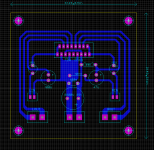
The example shown in the thread "An oversight on a TDA1554q pcb layout" at http://www.diyaudio.com/forums/chip-amps/247519-oversight-tda1554q-pcb-layout.html incorporates several of my suggestions.Not at all familiar with this chip but here are my thoughts.
Dale
Dale
My layout above was incorrect; it had the wrong footprint for U1. This required a total redesign. Here is the updated version.
Could you please attach the .sch file?
- Status
- This old topic is closed. If you want to reopen this topic, contact a moderator using the "Report Post" button.
- Home
- Design & Build
- Software Tools
- Help creating a pcb layout from schematics