I've had it in mind to do an update of my PCB layouts for the Phonoclone and VSPS projects. No large physical changes, just a clean up of the board design to the current "state of the art" i.e. my improved Eagle skills in working with polygon fills, restrict areas, etc.
I hate imperial, but when I started pretty all he components were based on 0.1" hole spacing, so it made sense, even though the board size was defined in cm, to make the layout working from a 50 micron grid.
Looking it at now, pretty much everything is metric, or purports to be.
If I was starting over again today, should I work from a cm or inch based grid?
If the board is in cm, should the mounting holes also be spaced in cm?
Finally, if mixing a cm board with an inch grid, what is the best way to keep the grid "centered" on the board area?
Any suggestions welcome - Thanks in advance
Richard
METRIC
Most components these days (SMD) are metric, and if you use BGA's its almost mandatory.
Metric is the international standard.
Look up IPC-7351 fast becoming the standard to use, and if you are new or even a jaded old hand at PCB's its the way to go.
http://www.dnu.no/arkiv1/The CAD Library of the Future.pdf
I still mostly use through hole, so do the layout in imperial, then switch to metric for placing dimensions and mounting holes. But I could quite easily work in ether format, and frankly, unless you have to interface with, say, an enclosure or mechanical design, I don't see it as being a great issue.
Most of the new components and probably 80+% of the worlds designs are now metric based. Even the SOIC is fast being replaced by smaller pitch 0.65mm and 0.5mm devices. A lot of the new components are bottom terminated devices these days, which again are metric pitch. These devices are going to become more common as they provide numerous advantages over more tradiytional packaging, ie no lead frame to add parasitic capacitance and inductance for signal integrity, excellent heat transfer away from silicon, via the copper slug, that becomes the thermal pad on the bottom of the device.
As stated earlier most (if not all BGA's) used in modern designs are based on a metric pitch.
More and more companies are moving towards using IPC-7351.
Pinkmouse, I cant remember when I did a PCB that wasn't going in some sort of enclosure, nearly all will be in enclosures/.
Ouroborous, I aslo use Cadstar. I use the 0.05mm grid that again is becoming common practice in the wider world. I guess you are using quite a few op-amps and logic in the old soic packages.
I have also been using Metric now for quite a few years.
So I would go metric, IIts easy to translate and update the components to the IPC-7351 standard, I have done a few libraries both in Cadstar and Allegro. Look at the PCB and electronic standard organisations that are behing metrification of PCB design.
http://www.smtnet.com/library/files/upload/The-Universal-PCB-Design-Grid-System.pdf
Most of the new components and probably 80+% of the worlds designs are now metric based. Even the SOIC is fast being replaced by smaller pitch 0.65mm and 0.5mm devices. A lot of the new components are bottom terminated devices these days, which again are metric pitch. These devices are going to become more common as they provide numerous advantages over more tradiytional packaging, ie no lead frame to add parasitic capacitance and inductance for signal integrity, excellent heat transfer away from silicon, via the copper slug, that becomes the thermal pad on the bottom of the device.
As stated earlier most (if not all BGA's) used in modern designs are based on a metric pitch.
More and more companies are moving towards using IPC-7351.
Pinkmouse, I cant remember when I did a PCB that wasn't going in some sort of enclosure, most will be packaged.
Ouroborous, I aslo use Cadstar. I use the 0.05mm grid that again is becoming common practice in the wider world. I presume you are using quite a few op-amps and logic in the old soic packages.
I have been using Metric now for quite a few years, and when interfacing with the 3D world via IDF (again with packing densities all products are built up virtualy in 3D land).
So I would go metric, Its easy to translate and update the components to the IPC-7351 standard, I have done a few libraries both in Cadstar and Allegro. Look at the PCB and electronic standard organisations that are behind metrification of PCB design.
http://www.smtnet.com/library/files/upload/The-Universal-PCB-Design-Grid-System.pdf
Some excellent links to white papers from the Mentor site.
http://www.mentor.com/products/pcb-system-design/techpubs/the-universal-pcb-design-grid-system-58117
Another excellent source of information for ALL things PCB is the IPC
http://www.ipc.org/Default.aspx
87% of ridgid PCBs are now produced in Aisa, the majority of these boards now are either 100% SMD (phones PC's, Apple products etc) or have a few connectors and instrusively reflowed through hole components. (6.7% North America, 5.2% Europe). China is top of the league with 40% of world production.
90% of flexis are produced in Aisa.
CEM basewd (very cheep) products account for 5% of world production, about 11% of boards are 2 layers PCB's, 13% are IC interposters (BGA / LGA devices etc), 10% Flexis, that leaves 61% of world wide PCB production in 2010 was multi-layer technology (included in here is HDI based designs, now reaching nearly 15%, (these are designs with 0.1mm laser drilled holes).
Above figure from the IPC World production report for 2010.
As stated earlier most (if not all BGA's) used in modern designs are based on a metric pitch.
More and more companies are moving towards using IPC-7351.
Pinkmouse, I cant remember when I did a PCB that wasn't going in some sort of enclosure, nearly all will be in enclosures/.
Ouroborous, I aslo use Cadstar. I use the 0.05mm grid that again is becoming common practice in the wider world. I guess you are using quite a few op-amps and logic in the old soic packages.
I have also been using Metric now for quite a few years.
So I would go metric, IIts easy to translate and update the components to the IPC-7351 standard, I have done a few libraries both in Cadstar and Allegro. Look at the PCB and electronic standard organisations that are behing metrification of PCB design.
http://www.smtnet.com/library/files/upload/The-Universal-PCB-Design-Grid-System.pdf
Most of the new components and probably 80+% of the worlds designs are now metric based. Even the SOIC is fast being replaced by smaller pitch 0.65mm and 0.5mm devices. A lot of the new components are bottom terminated devices these days, which again are metric pitch. These devices are going to become more common as they provide numerous advantages over more tradiytional packaging, ie no lead frame to add parasitic capacitance and inductance for signal integrity, excellent heat transfer away from silicon, via the copper slug, that becomes the thermal pad on the bottom of the device.
As stated earlier most (if not all BGA's) used in modern designs are based on a metric pitch.
More and more companies are moving towards using IPC-7351.
Pinkmouse, I cant remember when I did a PCB that wasn't going in some sort of enclosure, most will be packaged.
Ouroborous, I aslo use Cadstar. I use the 0.05mm grid that again is becoming common practice in the wider world. I presume you are using quite a few op-amps and logic in the old soic packages.
I have been using Metric now for quite a few years, and when interfacing with the 3D world via IDF (again with packing densities all products are built up virtualy in 3D land).
So I would go metric, Its easy to translate and update the components to the IPC-7351 standard, I have done a few libraries both in Cadstar and Allegro. Look at the PCB and electronic standard organisations that are behind metrification of PCB design.
http://www.smtnet.com/library/files/upload/The-Universal-PCB-Design-Grid-System.pdf
Some excellent links to white papers from the Mentor site.
http://www.mentor.com/products/pcb-system-design/techpubs/the-universal-pcb-design-grid-system-58117
Another excellent source of information for ALL things PCB is the IPC
http://www.ipc.org/Default.aspx
87% of ridgid PCBs are now produced in Aisa, the majority of these boards now are either 100% SMD (phones PC's, Apple products etc) or have a few connectors and instrusively reflowed through hole components. (6.7% North America, 5.2% Europe). China is top of the league with 40% of world production.
90% of flexis are produced in Aisa.
CEM basewd (very cheep) products account for 5% of world production, about 11% of boards are 2 layers PCB's, 13% are IC interposters (BGA / LGA devices etc), 10% Flexis, that leaves 61% of world wide PCB production in 2010 was multi-layer technology (included in here is HDI based designs, now reaching nearly 15%, (these are designs with 0.1mm laser drilled holes).
Above figure from the IPC World production report for 2010.
Last edited:
Marce.
Yes, a lot of my work is on Class-D Voice-Alarm/Public-Address amps. The analog side of these use SOIC8 op-amps, comparators and SOIC16 MOSFET gate drivers. The multi-channel amps have an embedded uP on the backplane board for control and monitoring. There's still quite a few SOIC logic chips on there as well as various TSSOP chips. As Eva said, a grid of 0.635mm (0.025") allows for most chips, with only a few dog-legs as the tracks connect to pins on the fine-pitch metric devices.
Yes, a lot of my work is on Class-D Voice-Alarm/Public-Address amps. The analog side of these use SOIC8 op-amps, comparators and SOIC16 MOSFET gate drivers. The multi-channel amps have an embedded uP on the backplane board for control and monitoring. There's still quite a few SOIC logic chips on there as well as various TSSOP chips. As Eva said, a grid of 0.635mm (0.025") allows for most chips, with only a few dog-legs as the tracks connect to pins on the fine-pitch metric devices.
Hi again, I pressed the wrong button during editing.
We use mainly the 0.65 and 0.5mm pitch devices, BGA's and QFNs etc, the soics are just to big for us now, our standard resistor is an (1005) 0402, as production wont let us go smaller. The boards I do are mainly 10-14 layer.
I have a set of IPC footprints in Cadstar Archive format if you want to look at some. I presume we will also have the same VAR, are you going to the engineering day at Telford?
Translation Table from Inch to Metric, I have a nicer PCB libraies version - via PM if anyone wantsit.
Inch to Metric Conversion Tables for PCB design Tom Hausherr's Blog
Oh sorry if I seem a bit zealus over this, but as the IPC figures show, we are loosing a lot of our manufacturing and design base in the West, and this upsets me, as over the last 25 years I have seen numerous firms I have worked for or done contracts for disapear. Interestingly Germay is still doing well with 2.1%, the UK is nowhere to be seen. Lack of investment, management, unions, a general undermining of Engineering in this country have all helped decimate our industrial heritage...
0603 as the standard R and C size for us! ( we hand solder the prototype boards). Our Cadstar system is really the second system here, as the company uses Mentor as the standard package. (though our CAD pcb guys much prefer Cadstar).
4-layer boards are the norm as well, so a lot less dense than yours.
4-layer boards are the norm as well, so a lot less dense than yours.
I miss the simpler boards, spent 8 years at a place and only got to 8 layers once (lots of soics and analogue, used imperial in thise days , and never thought I would change, wot a Luddite I was) , with SIV, length matching, having to use the interactive routers due to the complexities, the job has lost some of that relaxing feal that I use to get when routing. I still get to do the odd SMPS which I enjoy the most, as you can be quite creative with the copper, to try and keep EMC and all the other mush at bay. I'm lucky, we only go down to 0.8mm BGA's, I correspond with a couple of guys overseas that are ripping their hair out - 0.4mm pitch BGA's.
My mates just moved from here to a Manchester based mixing desk company and had to move to Pads, he's enjoying it, but would still prefer to be on good old Cadstar.
Just thought, you'll have access to all the 7351 stuff as Mentor bought Valour, who had bought PCB Libraries, who did a lot of the IPC-7351 stuff, and I believe Mentor are adding the tools to their products whilst doubling the price tio everyone else.
, and never thought I would change, wot a Luddite I was) , with SIV, length matching, having to use the interactive routers due to the complexities, the job has lost some of that relaxing feal that I use to get when routing. I still get to do the odd SMPS which I enjoy the most, as you can be quite creative with the copper, to try and keep EMC and all the other mush at bay. I'm lucky, we only go down to 0.8mm BGA's, I correspond with a couple of guys overseas that are ripping their hair out - 0.4mm pitch BGA's.My mates just moved from here to a Manchester based mixing desk company and had to move to Pads, he's enjoying it, but would still prefer to be on good old Cadstar.
Just thought, you'll have access to all the 7351 stuff as Mentor bought Valour, who had bought PCB Libraries, who did a lot of the IPC-7351 stuff, and I believe Mentor are adding the tools to their products whilst doubling the price tio everyone else.
Last edited:
Thanks to everyone who replied.
Alright, I'll give layout a re-spin starting from a 0.635mm grid. While my needs are far removed from the industrial applications being discussed later in this thread, going with metric from the ground up should solve a few of the nagging annoyances I ran into interfacing metric/imperial in past designs.
/r

Just for a bit of fun and info:
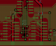
Its not often I use the 1.27mm pitch SOIC's these days, so I had to delve into an old design. These are 1.27mm SOIC's routed using the 0.05mm recommended grid. It is just for information, but as you can see It still looks neat, ie orthogonal tracks and 45® corners. With most EDA packages if you start the route from the pad it will put the first via or corner on a grid point that centres on the pad and on the 0.05mm grid. If you did it the other way the track would be slightly of centre of the pad, but still be acceptable.
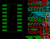
To show the contrast between SOIC's and some of today's components, the second picture shows a 16pin SOIC next to a bit of a DDR memory interface, the ball pitch is 0.1mm in the X and 0.8mm in the Y axis. The actual pads for the BGA are smaller than the vias (light green with grey drill hole), the finished hole size for the vias is 0.25mm, track and gap is 0.1/0.1mm. This is standard geometry these days with PC's etc, the next generation HDI gets even funkier.
http://www.pshk.org.hk/Activity DOC...chnologies/08 Miss Tarja Rapala 20.2.2009.pdf
Its not often I use the 1.27mm pitch SOIC's these days, so I had to delve into an old design. These are 1.27mm SOIC's routed using the 0.05mm recommended grid. It is just for information, but as you can see It still looks neat, ie orthogonal tracks and 45® corners. With most EDA packages if you start the route from the pad it will put the first via or corner on a grid point that centres on the pad and on the 0.05mm grid. If you did it the other way the track would be slightly of centre of the pad, but still be acceptable.
To show the contrast between SOIC's and some of today's components, the second picture shows a 16pin SOIC next to a bit of a DDR memory interface, the ball pitch is 0.1mm in the X and 0.8mm in the Y axis. The actual pads for the BGA are smaller than the vias (light green with grey drill hole), the finished hole size for the vias is 0.25mm, track and gap is 0.1/0.1mm. This is standard geometry these days with PC's etc, the next generation HDI gets even funkier.
http://www.pshk.org.hk/Activity DOC...chnologies/08 Miss Tarja Rapala 20.2.2009.pdf
Attachments
Do the design rules of your company require the PCBs to have one test point (for the ICT) per node? We have to do this (and use two test points per node for resistors of less than 22R). This really is a huge burden when trying to get high density. We are not allowed to use via holes as test points either.
We use boundry scan, then where required we add the minimum amount of testpoints (well actually use Preditors Testpoint function to add the testpoints or mark vias as suitable probing points). The board with the DDR memory is 86 sq cm, has 3500 pads and 2300 connections, we just couldn't get the test points on or get a jig made that would allow us to probe all the points.
Its 2000 since I last did a board where the engineer wanted test points on every node (and on a 0.1inch grid), they were a pain as he wouldn't let us use vias. When the cost of testing the boards started to outweigh the cost of the product he was finaly made to change. Basicly we do functional circuit test (JTAG, boundry scan) both here (tactical communications and surveillance) and my last place of work, and have had no problems. It is the trend theses days as getting the nodes on a design with so many small components and lack of space is couter productive both in finding problems and cost.
Its 2000 since I last did a board where the engineer wanted test points on every node (and on a 0.1inch grid), they were a pain as he wouldn't let us use vias. When the cost of testing the boards started to outweigh the cost of the product he was finaly made to change. Basicly we do functional circuit test (JTAG, boundry scan) both here (tactical communications and surveillance) and my last place of work, and have had no problems. It is the trend theses days as getting the nodes on a design with so many small components and lack of space is couter productive both in finding problems and cost.
- Status
- This old topic is closed. If you want to reopen this topic, contact a moderator using the "Report Post" button.
- Home
- Design & Build
- Software Tools
- not-so-newbie Eagle question : metric or imperial?