Re: Re: sophisticated amplifiers and simulation
It's Edmond.
Bob Cordell said:Hi Edmund,
It's Edmond.
Re: Re: sophisticated amplifiers and simulation

Cheers, Edmond.
Bob Cordell said:Hi Edmund,
First, no offense taken.
Second, I realize that when I say SPICE simulation results don't count, there are many caveats. You are pointing out situations where they DO count, and I agree with that. They especially count in moving one in the desired direction and giving perspective on what works better.
Originally posted by Bob Cordell However, I just stop short of believing a bottom-line result on distortion in an absolute sense because there are so many factors that can influence that bottom line that may not be adequately modeled. SPICE is a great tool, and I love it, but most would agree that we recognize its limitations and don't depend on it exclusively. Those who throw it out completely because it doesn't do everything are no wiser than those who depend on it exclusively. I'm sure you agree that the middle ground is where it is at.
Cheers,
Bob
Cheers, Edmond.
Re: Re: Re: Re: Re: Re: Re: Re: sophisticated amplifiers
Hi Glen,
This time and only this time, the honorable Douglas Self was talking through his hat.
His conclusions about MOSFET's were only base on stone aged SPICE models, which totally ignores the exponential gm of the so called weak inversion. Therefore his jagged graphs are quite misleading.
Besides, gm alone is not a good figure of merit, what counts is the product of gm and the effective impedance.
As these two parameters are quite different in nature, this also implies that you cannot blindly replace BJT's by MOSFET's, if the design is optimized for BJT's, and then complaining about the lesser performance. Designing a good MOSFET output stage demands a different approach.
Cheers, Edmond.
PS: I do have that article in EW+WW, but I don't send it to Bob, as it will certainly damage my reputation.")
G.Kleinschmidt said:Care to eleborate a bit? The non linearity of Vgs vs Id causes significant large signal distortion.
"The use of power FETs in output stages is often advocated. However, after much investigation, I have found the conclusion inescapable that FETs suffer not only from poor basic linearity, due to low gm, but also a crossover region that is inherently more jagged than BJTs. It is not possible to explore this in detail here, but see [7],[8] "............
7] Self, D "Audio Power Amplifier Design Handbook." Newnes 1996, p231. ISBN 0-7506-2788-3 (poor FET linearity)
8] Self, D "FETs vs BJTs- the linearity competition." Electronics & Wireless World, May 1995 p387. (poor FET linearity)
Above from here:
http://www.dself.dsl.pipex.com/ampins/dipa/dipa.htm#R
Any charitable soul out there with a copy of ref #8 to send to Bob Cordell? He's a poor misguided FET user who needs educating.
Cheers,
Glen

Hi Glen,
This time and only this time, the honorable Douglas Self was talking through his hat.
His conclusions about MOSFET's were only base on stone aged SPICE models, which totally ignores the exponential gm of the so called weak inversion. Therefore his jagged graphs are quite misleading.
Besides, gm alone is not a good figure of merit, what counts is the product of gm and the effective impedance.
As these two parameters are quite different in nature, this also implies that you cannot blindly replace BJT's by MOSFET's, if the design is optimized for BJT's, and then complaining about the lesser performance. Designing a good MOSFET output stage demands a different approach.
Cheers, Edmond.
PS: I do have that article in EW+WW, but I don't send it to Bob, as it will certainly damage my reputation.
Re: Re: Re: Re: Re: Re: Re: Re: Re: sophisticated amplifiers

Yes, I know the D.Self treatise on MOSFET linearity wasn't as good as it could have been and raises many issues for debate(that's why I cited it in the cheeky manner I which I did ). However, I still think that his point that the intrinsic linearity of MOSFET's as source followers is generally worse than that of BJT's as emitter followers is valid.
0.5% THD is still quite high, especially @ 100W into an 8 ohm load with 5 parallel MOSFET pairs in class A.
Bob, your 50W MOSFET design, without the EC, I believe, produced a THD-20 of 0.02% with about 40dB NFB.
As a comparison, D. Self's EF output 'blameless' does about 0.01% THD-20 with less NFB (miller compensation), using a single pair of 2MHz fT BJT's in a 30W design.
Cheers,
Glen
estuart said:
Hi Glen,
This time and only this time, the honorable Douglas Self was talking through his hat.
His conclusions about MOSFET's were only base on stone aged SPICE models, which totally ignores the exponential gm of the so called weak inversion. Therefore his jagged graphs are quite misleading.
Besides, gm alone is not a good figure of merit, what counts is the product of gm and the effective impedance.
As these two parameters are quite different in nature, this also implies that you cannot blindly replace BJT's by MOSFET's, if the design is optimized for BJT's, and then complaining about the lesser performance. Designing a good MOSFET output stage demands a different approach.
Cheers, Edmond.
PS: I do have that article in EW+WW, but I don't send it to Bob, as it will certainly damage my reputation.
Bob Cordell said:
Self was at least partially full of baloney on this one. At the very least, he had blinders on and did not tell the whole story. MOSFETs have about 10 times less gm at a given operating current than bipolars. If you get past this, they are every bit as linear. As a very rough approximation, the dynamic source resistance (1/gm) of a MOSFET is about 250/Id in mA.
Let's build a 100 W Class A amplifier from MOSFETS. It must support 40V pk and 5A pk into an 8 ohm load. Lets give it 44V main rails. The Class A idle bias must be 2.5 A. Lets use 5 pairs of MOSFET output devices, each carrying 500 mA of idle bias and each dissipating 22W at idle. The dynamic source impedance of each MOSFET is about 250/500 = 0.5 ohms. The five upper devices in parallel will yield a net upper Rs of 0.5/5 = 0.1 ohms. The bottom five devices will do the same, bringing the total open-loop output impedance at idle to 0.05 ohms.
At a peak current of 5 A, each of the upper transistors is at 1 amp with an Rs of 0.25 ohms. We have five in parallel, so we get an effective net Rs of 0.05 ohms. To first order, this is the same as at idle bias. Of course, there will be wiggles in between, and this approximation is only that, but the point is that the output stage net transconductance, variations of which will cause distortion, will actually vary very little with signal in this Class-A arrangement.
In any case, the variation in net 1/gm is certainly less than 0.04 ohms over signal. This is less than 0.5% of the 8 ohm load, suggesting in very rough terms open loop distortion on the order of less than 0.5%. Now we put 40 dB of NFB around it and we are at 0.005%, and actually probably quite a bit less.
Cheers,
Bob
Yes, I know the D.Self treatise on MOSFET linearity wasn't as good as it could have been and raises many issues for debate(that's why I cited it in the cheeky manner I which I did
). However, I still think that his point that the intrinsic linearity of MOSFET's as source followers is generally worse than that of BJT's as emitter followers is valid.0.5% THD is still quite high, especially @ 100W into an 8 ohm load with 5 parallel MOSFET pairs in class A.
Bob, your 50W MOSFET design, without the EC, I believe, produced a THD-20 of 0.02% with about 40dB NFB.
As a comparison, D. Self's EF output 'blameless' does about 0.01% THD-20 with less NFB (miller compensation), using a single pair of 2MHz fT BJT's in a 30W design.
Cheers,
Glen
Re: Re: Re: Re: Re: sophisticated amplifiers
Nice simulation job! The changes you mentioned should not make a really big change in the behvior of the amplifier, so these simulations should be reasonably relevant.
Where did you get the SPICE models for the 2sk1530 and the 2sj201. If you can, please email me a copy of them at bob@cordellaudio.com.
Thanks,
Bob
estuart said:
Hi Bob,
I made a small mistake. 7ppm refers to a slightly different version of your amp, i.e. 2 pair of MOSFETs (they were superimposed on each other, so I overlooked it). Furthermore, the main power supply was +/- 40V in stead of 35V and Po was 85W in stead of 50W.
Here are more correct figures, although with 2SK1530/2SJ201 in stead of IRFxxx:
THD @ 20kHz and a measuring bandwidth of 200kHz
Po = 0.5W -> 1.45ppm
Po = 5W -> 4.16ppm
Po = 50W -> 6.24ppm
As you can see, my simulator is quite in his element when sniffing at your amp.
Cheers, Edmond
Nice simulation job! The changes you mentioned should not make a really big change in the behvior of the amplifier, so these simulations should be reasonably relevant.
Where did you get the SPICE models for the 2sk1530 and the 2sj201. If you can, please email me a copy of them at bob@cordellaudio.com.
Thanks,
Bob
GOODWILL, Good Name, Flags - symbols of your Activity
Nelson & Bob ( what a team!work )
In this proposed HEXFET amp output Class A of Bob (5 parallel MOS complementary),
which actual devices are everybody using.
To produce these test records?
Nelson says IRF9xxx ... is this the usual IRF9610 ??
... I do not see any other actual transistors
... besides Bob asking to get SPICE of 2sk1530 and the 2sj201, in his private Email
Why not publish SPICE Model
for all members of www.diyaudio.com
I usually have put my models inside a
<Quote>
spice model
spice modle
</Quote>
this is what we other do on regular basis
what is the hook here - Me Lineup, see no hook ...
Hope to get a few answers to inform me better.
Thanks & Regards to Our masters, sharing their 'in dept discussion'
lineup - stands for, I hope, Good-Will & Frank-ness
- out with it, in the open
- the only thing the will hold, in the long run
- is to be as open as you can
- with what knowledge you have earned
------------------------------------------
------------------------------------------
APPENDIX A.
Basic Lesson #1 of Marketing Symbols & Good will.
The Actual Bottomline here is
Good Public Relations - to all diy audio people of this world.
From Canada in west - to Shanghai, Tokyo & Dehli in the east.
A good NAME, Your good will shown = GOODWILL, is better than money.
A bad name ( BadWill, will not give good money, in the long run.
You may have heard about the value of Brand, Trademark & Logos
.. and what they can represent.
Name, your LABEL, It is the Flag of your Activity ...
'lineup' it stands for something, represents a whole bunch of matters,
like Union Jack & Star's & Stripes & The NaziFlag
... it can for people be something positive / negative
... But !!!
This is NOT a static Value !!!!!!!
... it changes dependent on What the people using this Trademark
are up to and are actually doing/saying.
It is the same with symbols like World trade Center & Statue Of Liberty.
They can represent different values and these values
as seen from a perspective of The total world's populations
can change, rather quickly, at times.
The Naziflag was actually first a symbol of success.
It was admired by many, not only Germans,
until things began to unfold.
----------------------
Nelson Pass Labs - this makes people associate.
Today, it represents HIGH Quality, Craftsmanship and great Positives to most all DiyAudio Community.
And I forsee no change at all in this specific case
----------------------
It is like with Money.
There can be an Inflation or Reflation of value.
If Nelson would start massproduction of cheap and low quality audio amps,
you should soon, as a few years passed by, see a change in people minds.
.... You better believe me.
I tell no lies & I do no unnecessary sweet talk here.
Nelson Pass said:
I only recall that the Harris and Fairchild had a flat transconductance
across the audio band - I failed to note the absolute values.
------------------
I conclude that we are probably looking at a drop off from spec.
Nelson & Bob ( what a team!work )
In this proposed HEXFET amp output Class A of Bob (5 parallel MOS complementary),
which actual devices are everybody using.
To produce these test records?
Nelson says IRF9xxx ... is this the usual IRF9610 ??
... I do not see any other actual transistors
... besides Bob asking to get SPICE of 2sk1530 and the 2sj201, in his private Email
Why not publish SPICE Model
for all members of www.diyaudio.com
I usually have put my models inside a
<Quote>
spice model
spice modle
</Quote>
this is what we other do on regular basis
what is the hook here - Me Lineup, see no hook ...
Hope to get a few answers to inform me better.
Thanks & Regards to Our masters, sharing their 'in dept discussion'
lineup - stands for, I hope, Good-Will & Frank-ness
- out with it, in the open
- the only thing the will hold, in the long run
- is to be as open as you can
- with what knowledge you have earned
------------------------------------------
------------------------------------------
APPENDIX A.
Basic Lesson #1 of Marketing Symbols & Good will.
The Actual Bottomline here is
Good Public Relations - to all diy audio people of this world.
From Canada in west - to Shanghai, Tokyo & Dehli in the east.
A good NAME, Your good will shown = GOODWILL, is better than money.
A bad name ( BadWill, will not give good money, in the long run.
You may have heard about the value of Brand, Trademark & Logos
.. and what they can represent.
Name, your LABEL, It is the Flag of your Activity ...
'lineup' it stands for something, represents a whole bunch of matters,
like Union Jack & Star's & Stripes & The NaziFlag
... it can for people be something positive / negative
... But !!!
This is NOT a static Value !!!!!!!
... it changes dependent on What the people using this Trademark
are up to and are actually doing/saying.
It is the same with symbols like World trade Center & Statue Of Liberty.
They can represent different values and these values
as seen from a perspective of The total world's populations
can change, rather quickly, at times.
The Naziflag was actually first a symbol of success.
It was admired by many, not only Germans,
until things began to unfold.
----------------------
Nelson Pass Labs - this makes people associate.
Today, it represents HIGH Quality, Craftsmanship and great Positives to most all DiyAudio Community.
And I forsee no change at all in this specific case ----------------------
It is like with Money.
There can be an Inflation or Reflation of value.
If Nelson would start massproduction of cheap and low quality audio amps,
you should soon, as a few years passed by, see a change in people minds.
.... You better believe me.
I tell no lies & I do no unnecessary sweet talk here.
Re: Re: Re: Re: Re: Re: sophisticated amplifiers
Thanks Bob.
The models are home brew and running only under Micro-Cap V8. They are partly based on the BSIM3 model (level 8) and partly on a couple of diodes representing Cgd and Cds.
Which simulator you are using? If it's LT-Spice for example, I'm afraid my models are of no use to you.
Please, let me know.
Cheers, Edmond.
Bob Cordell said:Nice simulation job! The changes you mentioned should not make a really big change in the behvior of the amplifier, so these simulations should be reasonably relevant.
Where did you get the SPICE models for the 2sk1530 and the 2sj201. If you can, please email me a copy of them at bob@cordellaudio.com.
Thanks,
Bob
Thanks Bob.
The models are home brew and running only under Micro-Cap V8. They are partly based on the BSIM3 model (level 8) and partly on a couple of diodes representing Cgd and Cds.
Which simulator you are using? If it's LT-Spice for example, I'm afraid my models are of no use to you.
Please, let me know.
Cheers, Edmond.
Re: Re: Re: Re: Re: Re: Re: sophisticated amplifiers
Hi Edmond,
Thanks. Yes, I use LTSPICE. Oh, well...
Cheers,
Bob
estuart said:
Thanks Bob.
The models are home brew and running only under Micro-Cap V8. They are partly based on the BSIM3 model (level 8) and partly on a couple of diodes representing Cgd and Cds.
Which simulator you are using? If it's LT-Spice for example, I'm afraid my models are of no use to you.
Please, let me know.
Cheers, Edmond.
Hi Edmond,
Thanks. Yes, I use LTSPICE. Oh, well...
Cheers,
Bob
Re: Re: Re: Re: Re: Re: Re: sophisticated amplifiers
Hi Edmond,
LTSpice supports BSIM3 level 8. If your model is just a subcircuit containing a BSIM3 model combined with two diodes as you say, it should be able to be adapted to LTSpice quite easily. All that's needed are text files with the BSIM3 and diode parameters and of course, knowing which diode is which.
If you have these, I could hook them up to an LTSpice symbol file (.asy) so the symbol representing the device would be draggable onto the schematic and use the appropriate subcircuit automatically.
estuart said:The models are home brew and running only under Micro-Cap V8. They are partly based on the BSIM3 model (level 8) and partly on a couple of diodes representing Cgd and Cds.
Which simulator you are using? If it's LT-Spice for example, I'm afraid my models are of no use to you.
Hi Edmond,
LTSpice supports BSIM3 level 8. If your model is just a subcircuit containing a BSIM3 model combined with two diodes as you say, it should be able to be adapted to LTSpice quite easily. All that's needed are text files with the BSIM3 and diode parameters and of course, knowing which diode is which.
If you have these, I could hook them up to an LTSpice symbol file (.asy) so the symbol representing the device would be draggable onto the schematic and use the appropriate subcircuit automatically.
andy_c said:[snip]
In an email, Edmond mentioned that the Cgs values appeared to be low. I had a cursory look at them and this does appear to be the case.
[snip]
Hi Andy,
Meanwhile, I had a closer look at some (old) test circuits and the CGS cap between node 3 and 5 is NOT the real input capacitance, rather a correction term to make Ciss at Vds=30V exactly equal to the value in the data sheet. The bulk of Ciss is (apparently) derived from the geometric parameters of the BSIM3 model.
Anyhow, I think it's wise to make some LT-Spice test circuits too, and check if the capacitances are in accordance with the data sheet.
Cheers, Edmond
estuart said:Meanwhile, I had a closer look at some (old) test circuits and the CGS cap between node 3 and 5 is NOT the real input capacitance, rather a correction term to make Ciss at Vds=30V exactly equal to the value in the data sheet. The bulk of Ciss is (apparently) derived from the geometric parameters of the BSIM3 model.
Anyhow, I think it's wise to make some LT-Spice test circuits too, and check if the capacitances are in accordance with the data sheet.
Hi Edmond,
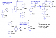
I've done some capacitance sims and the Cgs of the device is indeed much higher than the external capacitance added in the subcircuit, just as you say. I have never studied the BSIM3 model, so at the present time I have no clue how the internal capacitances of this model get calculated. The circuit below shows three simulations - the first for Cgs, the second for Cgd, and the third for Ciss as a sanity check to make sure the computed Cgs and Cgd add up to Ciss. DC drain currents in all three circuits are 150 mA, and the DC value of Vdg is 30V in each case.
The first circuit (FET=U1) bootstraps the drain voltage so the total instantaneous Vdg is a constant 30V. This eliminates Cgd. The bandwidth at G1 is calculated, and Cgs is computed from the gate resistance and the -3dB frequency at G1.
The second circuit (FET=U2) bootstraps the source so that the total instantaneous Vgs is a constant 1.883 V, the voltage required to get 150 mA drain current. This eliminates Cgs. The bandwidth at G2 is calculated, and Cgd is computed from the gate resistance and the -3dB frequency at G2.
The final circuit (FET=U3) just grounds the source, sets the DC gate voltage to 1.883V and the DC drain voltage to 30V above the gate. The bandwidth at G3 is calculated, and Ciss is again computed from the gate resistance and the -3dB frequency at G3.
This was done for the 2SK1530 and the 2SJ201. The results are as follows:
2SK1530: Cgs = 698pF, Cgd = 103pF (Vdg = 30V and Vgs = 1.883V)
2SJ201: Cgs = 1120pF, Cgd = 231pF (Vgd = 30V and Vgs = -1.937V)
Attachments
andy_c said:Hi Edmond,
I've done some capacitance sims and the Cgs of the device is indeed much higher than the external capacitance added in the subcircuit, just as you say. I have never studied the BSIM3 model, so at the present time I have no clue how the internal capacitances of this model get calculated. The circuit below shows three simulations - the first for Cgs, the second for Cgd, and the third for Ciss as a sanity check to make sure the computed Cgs and Cgd add up to Ciss. DC drain currents in all three circuits are 150 mA, and the DC value of Vdg is 30V in each case.
The first circuit (FET=U1) bootstraps the drain voltage so the total instantaneous Vdg is a constant 30V. This eliminates Cgd. The bandwidth at G1 is calculated, and Cgs is computed from the gate resistance and the -3dB frequency at G1.
The second circuit (FET=U2) bootstraps the source so that the total instantaneous Vgs is a constant 1.883 V, the voltage required to get 150 mA drain current. This eliminates Cgs. The bandwidth at G2 is calculated, and Cgd is computed from the gate resistance and the -3dB frequency at G2.
The final circuit (FET=U3) just grounds the source, sets the DC gate voltage to 1.883V and the DC drain voltage to 30V above the gate. The bandwidth at G3 is calculated, and Ciss is again computed from the gate resistance and the -3dB frequency at G3.
This was done for the 2SK1530 and the 2SJ201. The results are as follows:
2SK1530: Cgs = 698pF, Cgd = 103pF (Vdg = 30V and Vgs = 1.883V)
2SJ201: Cgs = 1120pF, Cgd = 231pF (Vgd = 30V and Vgs = -1.937V)
Hi Andy,
Cgs is a bit lower than the Toshiba specs, but these were measured at Vgs=0. So, would you be so kind to run some more simulations, now at Vgs=0?
Apologies for my 'laziness', but I'm unfamiliar with LT-Spice, that's why I'm asking you.
Cheers, Edmond.
Re: BS
Hi Edmond,
Sure, no problem. The results are:
2SK1530: Cgs = 886pF @ Vgs=0, Vds=30V
2SJ201: Cgs = 1439pF @ Vgs=0, Vds=30V
BTW, the Berkeley BSIM models look pretty comprehensive. Sub-threshold conduction, woo woo! There was no documentation on them in the LTSpice help, but I found a whole lot of stuff at the Berkeley BSIM web site. I downloaded the manual for BSIM 3v3. It's 205 pages! Yow.
Andy
estuart said:
Hi Andy,
Cgs is a bit lower than the Toshiba specs, but these were measured at Vgs=0. So, would you be so kind to run some more simulations, now at Vgs=0?
Apologies for my 'laziness', but I'm unfamiliar with LT-Spice, that's why I'm asking you.
Hi Edmond,
Sure, no problem. The results are:
2SK1530: Cgs = 886pF @ Vgs=0, Vds=30V
2SJ201: Cgs = 1439pF @ Vgs=0, Vds=30V
BTW, the Berkeley BSIM models look pretty comprehensive. Sub-threshold conduction, woo woo! There was no documentation on them in the LTSpice help, but I found a whole lot of stuff at the Berkeley BSIM web site. I downloaded the manual for BSIM 3v3. It's 205 pages! Yow.
Andy
AndrewT said:When are you two guys going to colaborate on writing a beginner's Wiki, an intermediate Wiki and an advanced Wiki on using/setting up simulators?
Hi AndrewT,
I noticed in another thread that you began using SPICE and were having some problems. SPICE itself is a huge topic about which entire books have been written. Then there's the quirks that each individual program UI has. When starting out, it's best to start simple - like finding the step response of an RC low-pass filter or the like. Try to do some things, then when you get stuck, just ask.
AndrewT said:When are you two guys going to colaborate on writing a beginner's Wiki, an intermediate Wiki and an advanced Wiki on using/setting up simulators?
I did find an LTSpice tutorial here that might be useful to you. I'm getting off-topic here, but one idea might be to start something like an "Absolute Beginner to SPICE" thread. I'd be willing to help with questions in such a thread if LTSpice were the chosen tool (I don't know the UI of other tools). LTSpice is a logical choice because it's free, used by many people, and has no circuit size limitations.
andy_c said:
I did find an LTSpice tutorial here that might be useful to you. I'm getting off-topic here, but one idea might be to start something like an "Absolute Beginner to SPICE" thread. I'd be willing to help with questions in such a thread if LTSpice were the chosen tool (I don't know the UI of other tools). LTSpice is a logical choice because it's free, used by many people, and has no circuit size limitations.
Thanks guys for your continued efforts here. Such a thread might be a really good idea. I've used SPICE since its inception (BTW, does anyone remember SLIC by Bill McCallugh?), but I have never considered myself to be a sophisticated user of it, so I'd be happy to contribute some dumb questions. I'm particularly inexperienced with the details of models and packaging them in subcircuits.
Having suffered many years with SPICE in batch mode with line-printer outputs running on IBM 370 and VAX 11/780 machines, I concur that LTSPICE is a gift from heaven. I can't imagine why it would not be the defaco simulator of choice for DIY.
Thanks,
Bob
Bob Cordell said:[snip]
Having suffered many years with SPICE in batch mode with line-printer outputs running on IBM 370 and VAX 11/780 machines, I concur that LTSPICE is a gift from heaven. I can't imagine why it would not be the defaco simulator of choice for DIY.
Thanks,
Bob
Hi Bob,
On this forum it has already been declared as the de facto standard, although it's not my preferred tool. It seems that it has something to do with $$$.
Cheers, Bob.
Hi Andrew T
Are you saying that you haven't used SPICE yet?
You could try SIMETRIX which has a free evaluation version and runs transistor circuits up to about 30 devices. I believe you can download it from their web site.
It has tuition examples.
But the important thing to remember is that - if the computer says something does not work it is probably right. If it says something works, check it!
cheers
John
Re: Re: Re: Re: Re: Re: Re: Re: Re: I repeat my Request
No I did not miss them, i just didn't see the point in answering a lot of pointless questions.
1) BJT are 2SA1386/2SC3518. I mistakenly referred to these earlier as 35/60 MHz. They are infact 40/50MHz.
2) Yes I did build an measure a complete output stage in isolation. How do you think I measured the output stage THD?
3) I didn't get spice models for the Sanken BJT's and my output-stage conclusions are not based of SPICE simulation.
I have already given you a brief showing of the design, and, as it progresses, the entire thing will be published (allowing scrutiny) on my website in full. Right now, I finishing of the schematics in .GIF format.
You'll just have to wait for it.
Cheers,
Glen
Bob Cordell said:
Hi Glen,
Perhaps you missed my questions here from an earlier post.
Thanks,
Bob
No I did not miss them, i just didn't see the point in answering a lot of pointless questions.
1) BJT are 2SA1386/2SC3518. I mistakenly referred to these earlier as 35/60 MHz. They are infact 40/50MHz.
2) Yes I did build an measure a complete output stage in isolation. How do you think I measured the output stage THD?
3) I didn't get spice models for the Sanken BJT's and my output-stage conclusions are not based of SPICE simulation.
I have already given you a brief showing of the design, and, as it progresses, the entire thing will be published (allowing scrutiny) on my website in full. Right now, I finishing of the schematics in .GIF format.
You'll just have to wait for it.
Cheers,
Glen
Re: Re: Re: Re: Re: Re: Re: Re: Re: Re: I repeat my Request
Hi Glen,
The questions were not pointless.
What value of THD did you get for the output stage at 20 kHz full power? You did not answer this one.
Am I correct in believing that full power is 500W into 8 ohms, driven balanced from both sides?
What kind of a source did you use in order to develope the necessary very large balanced drive signals to measure the output stage in isolation? It would seem like a pretty big undertaking to measure such a large, high-power output stage.
Since the output stage is Class-A, I assume that you would have also had to build the balanced rail-tracking amplifier that feeds its floating rails in order to test it, no?
Cheers,
Bob
G.Kleinschmidt said:
No I did not miss them, i just didn't see the point in answering a lot of pointless questions.
1) BJT are 2SA1386/2SC3518. I mistakenly referred to these earlier as 35/60 MHz. They are infact 40/50MHz.
2) Yes I did build an measure a complete output stage in isolation. How do you think I measured the output stage THD?
3) I didn't get spice models for the Sanken BJT's and my output-stage conclusions are not based of SPICE simulation.
I have already given you a brief showing of the design, and, as it progresses, the entire thing will be published (allowing scrutiny) on my website in full. Right now, I finishing of the schematics in .GIF format.
You'll just have to wait for it.
Cheers,
Glen
Hi Glen,
The questions were not pointless.
What value of THD did you get for the output stage at 20 kHz full power? You did not answer this one.
Am I correct in believing that full power is 500W into 8 ohms, driven balanced from both sides?
What kind of a source did you use in order to develope the necessary very large balanced drive signals to measure the output stage in isolation? It would seem like a pretty big undertaking to measure such a large, high-power output stage.
Since the output stage is Class-A, I assume that you would have also had to build the balanced rail-tracking amplifier that feeds its floating rails in order to test it, no?
Cheers,
Bob
- Home
- Design & Build
- Software Tools
- Spice simulation