example 2 TDA1541
An example of dac with two tda1541 :
http://cdp101.hp.infoseek.co.jp/dasr1/dasr1.html
An example of dac with two tda1541 :
http://cdp101.hp.infoseek.co.jp/dasr1/dasr1.html
Hi,
A SONY with two times TDA1541 ??? Or did they modify the SONY a bit ??
Cant read the text, pitty..! I wonder how they did the splitting, probably by
the digital filter (smd underside of pcb?? or on a backplane ?,
there is not much logic on the board)
The clock doesn't seem to be a fancy one (xtal+'04)
Anyway,
I am working on such a DAC, NOS mode! Status now is that i ordered one board
to be made, i am waiting for it. Hopefully i get it before Xmas. Splitting I2S
into left and right can be done with:
- one 4517 shift register
- one GAL20V8 programmed with some logic.
If you want to have the I2S towards one DAC to be differential, you also need
one '74 flipflop.
In my design i also included a master clock in the DAC (G.Tent clock) and a
fifo register to buffer the incoming I2S stream. I am going for I2S in, not spdif.
But a spdif receiver in front of the DAC should be possible.
Clock is 11.xx MHz, the clock is fed back to an old CD player where i get my I2S.
Not on the board: powersupplies and analog output. If i make progress, i will do
some posting.
The splitting was already posted here (using many 74xxx shift registers). Now it
is one 4517. The old page is here http://www.home.zonnet.nl/baltusg/I2S.html
many logic chips, but it works!!
There will be a follow-up next year,
Guido B.
So i can easily make changes and i did not make my mind up yet.
The digital part can't be tweaked so much as the analogue part.
Differential mode or not, trannie, tube output, fets, ?????
Also the supply: 3 leg thing, discreet, whatever ??
Anyway, out of the country for a few days. Back somewhere next week.
Groetjes,
Guido B.
The digital part can't be tweaked so much as the analogue part.
Differential mode or not, trannie, tube output, fets, ?????
Also the supply: 3 leg thing, discreet, whatever ??
Anyway, out of the country for a few days. Back somewhere next week.
Groetjes,
Guido B.

Hi,
Looks are really nice indeed! But that doesn't count...
Sound..? Don't know yet, first need proper power supply,
proper output stage and a proper way to get i2s from cd
player to dac (and the clock reversed). So that is still
a long time from now.
Schematic..? When all works well, i'll post it. It involves programmable logic (GAL20V8).
First i need to do basic testing, for that i am still waiting for one
component..
Decouplingcaps are 0.33uF Siemens polyester film, but there
is room for other types (but not the megahuge types). I don't know your experts, but
other experts think the wima mks 4 is not so good. Than again, i am not an expert.
Had some request already for pcb's.. When all works well, i am going to see if i can
have other people order directly from the pcb factory. I paid 39 euro, but it will be less
for others (films are ready). You have to be patient there. If you are interested, you better
start looking for a GAL programmer. I have one, that's why i am using it.
Guess half the pcb could be used to sent 'mono' I2S to other DAC's. Using a saw is all it takes..
But only non-os, otherwise the freq will be to high for the dig. logic (4517 is slow).
Or put two dig filters behind the splitting part :->
More to come in the future.
BTW,
I am not Guido Tent, allthough i am using one of his clocks on this pcb.
Why? It is small and easy to implement. But it is possible to use an external clock
Already tested the clock part, the cd player works with the clock on the pcb.
If i only had that reset IC....
Greetings,
Guido B.

Hi,
Faked the reset IC with a switch. And.....
Got it working (after some reprogramming of the GAL) :-> !!
Seems the only thing wrong is that i forgot a resistor on the reset line to one IC (delayed with a cap, but the input is giga-ohm, so the cap is not discharged). A minor thing so to say.
Now i have to start looking at all the output circuits out there on the net, powersupply and a proper connection with the CD player.
Got it working by using a I/V opamp conversion circuit :-(.
The 'Eringa CD filter' some dutch people might now.. It has similar circuits as original philips players have, but only much better components (OP44, relais for mute and de-emphasis, polystyrene and big output caps). Something from the end of the eighties.. But it works.
Keep you posted,
Guido
part1
Hi,
The schematics. This is NOT a complete DAC, only the first part of it. Missing is power-supply, output circuit and connection to CD player. DAC is non-oversampling two times TDA1541A with one for left and one for right channel (differential possible). The DAC
has an own clock and the clock is fed back to the CD player. Between CD player and DAC sits a FIFO register to avoid synchronisation problems.
The used FIFO (U7) has asynchronious write and read, the incoming I2S clock is used to write to the FIFO, the DAC clock is used to read it. The used FIFO has 2k of memory, but it does not really matter if it is more or less. It was the cheapest dip fifo i could get. (this chip is from CYPRESS and is an AM72xx (AMD) clone, any dip version should work).
The empty flag and half-full flags are used to stop/start reading of the FIFO. I'll come back to this. The I2S WS and datalines just go in at the left side and appear again on the right side. It does not take long to go through the 2048 memory-cells at a clockrate of 2.8 MHz :->. I choosed D3 and D8 on U7 for layout reasons.
The buffer U2 is used to make pin 1 (write enable) high during reset with R1. D1 and C8 are used to delay this (pin WE needs to stay high for 25 nanosec after reset becomes high, value depending on FIFO type). Since the G input of the buffer is not really discharging C8, i need to parallel it with a resistor (not in the schematics yet). My only mistake (?).
I don't have the MAX707 yet, so i haven't tested it all. Using a double switch now to emulate the reset chip. Also on this page are the de-coupling caps for the digital part.
Attachments
part2
This page is more complicated....
On the top right X1, a 11.2896 MHz crystal (G.Tent's). It goes to U9, which divides the clock by 2 and 4. JP12 is used to feed the 11MHz to the CD-player (old philips player with SAA7210 inside where i get my I2S). If JP10/11 are disconnected, JP12 can also
be used to feed an external clock to U9. So other clocks could be used, i myself might try others later.
It is important to feed the clock back to the CD player !!! (to the SAA7210 or, like i did to keep the dig. out, to the SAA7220) If it is not the same, the freq will differ a little bit in the player compared to the DAC. Then the FIFO will run full or empty, depending on
which clock is faster. U9 feeds 5.6MHz (div2) and 2.8MHz (div4) to the GAL.
Looking at the I2S signals, the left frame is first on the dataline and then the right frame. If we look halfway the transmission, the wordselect line is going high to indicate that the right frame is on the dataline. If we now invert the wordselect signal, the DAC will think it is the left frame. So we feed the inverted wordselect signal and the dataline to the right DAC. For the left DAC we need the left frame, which was there 32 clockcycles ago.
Therefore the dataline is fed into a 32 bit shiftregister and the output is used to feed the left DAC. 32 clockcycles later the inverted wordselect signal will indicate to the DACs that the right frame is coming in. Since we want to put the same data on the line, we need to delay both frames. The right frame is already delayed by the shiftregister, so we have that. The left frame is delayed again with a second 32 bit shiftregister, so we have all.
U6 is this shift register. A synchronious fifo so to say with a memory of 64 cells and a tap between cell 32 and 33. A frame is 32 bit (16 bit unused), i think this is the samefor the SAA7210 and a Crystal receiver like the CS8412.
E.g. the SAA7220 is only 16 bit. But using the oversampling filter will NOT work, the clock is 5.6MHz and this is too high for U6 (the clock is only doubled, but since the words are only 16 bit, the total number of frames is times four, the 7220 is four times oversampling). During testing i had several brands of 4517, but only a Philips one worked!! The I2S clock to the DAC's (U8-pin17) is derived from the 2.8MHz. Also the clocking of the logic (U8-pin 21 and 22). The GAL contains:
CLOCK = CLKDIV4 ;equal
CLOCK_INV = /CLKDIV4 ;inverted
I2SCLK = /CLKDIV4 ;inverted
The clock from pin 21 is also used to latch the registered outputs of the GAL via pin1.... Registered outputs can be made registered by using ":=" in the declaration. This is used for data and ws (later). So the shift register and the GAL are both clocking on low to high. Strange? Well suppose the MSB just came out of the fifo, therefore it is available at pin6 of the GAL. It is also available at pin 9 of U6, the shift register.
Before clocking, the previous MSB will be in cell 32 of the register and available at pin10 of U6 and the MSB before at pin11. When clock goes low to high the GAL will therefore clock the MSB's: all is in sync. The logic clocks on the same clock, but some (in case of the 4517, many) nanoseconds later the data will be at the output pins. But then the correct bit is already clocked by the GAL.. Hihi. According to the databook, the holdtime after clock goes low to high is 0 nanosec minimum for the GAL. That's why this is possible.
The second frame to both DACs can be inverted to create a differential output. This is done by inverting the second frame to the DAC (not entirely correct, one LSB off!). So we need to know where the frame is. Since the word-select signal WSAB is running one clockcycle before the actual frame, we need to delay it with one cycle. This is done in two stages by flipflop U5. In order to choose to use differential output or not, one input from the GAL is used and another input is used to create a mute (data=low for all bits).
So now we can create the signals for the DACs:
WSL := /WS
WSR := /WS
Wordselect out is the inverted of wordselect in.
For data to the right DAC data and the 32 cycles delayed data are used: For data to the left DAC 32 cycles and 64 cycles delayed data are used. But '32 cycles delayed data' is not the same data! It depends where you are in time. This depends again on the WS signal.
The first two lines are used in normal mode (differential is high) and the first line and line 3 and 4 are used in differential mode.
If the data should be inverted in the second frame (WS low) depends if the frame is the second one or not, indicated by the delayed signal WSDELAY.
DATAR := WS * DATA * MUTE +
/WS * SHIFT32 * DIFFERENTIAL * MUTE +
/WS * SHIFT32 * /DIFFERENTIAL * WSDELAY * MUTE +
/WS * /SHIFT32 * /DIFFERENTIAL * /WSDELAY * MUTE
DATAL := WS * SHIFT32 * MUTE +
/WS * SHIFT64 * DIFFERENTIAL * MUTE +
/WS * SHIFT64 * /DIFFERENTIAL * WSDELAY * MUTE +
/WS * /SHIFT64 * /DIFFERENTIAL * /WSDELAY * MUTE
Now the FIFO reading, it needs to be done before the GAL/logic clocks in the data. Also read should be low during the time the output must be valid. If read is high, the data output switches off. Therefore a new 2.8 MHz clock is created wich is running 1/4 of a cycle before the clkdiv4 clock and is inverted. This is done by using clkdiv2 and clkdiv4.
The reading should start if the FIFO is neither full or empty. Therefore i use the half-full flag. The flags are fed to flipflop U4A. During reset, empty will be low and Q is forced low. When the fifo is filled empty will go high, but Q remains low. When the fifo is half-full, half will go low and Q will be made high. After this, Q will remain high untill the fifo is empty again. So now we have the read defenition for the fifo:
FIFOREAD = /GO + GO * CLKDIV2 * CLKDIV4 + GO * /CLKDIV2 * /CLKDIV4
If GO is low, FIFOREAD is high. So during reset it is high, that's required. If the FIFO has been half-full, GO is high and the fifo is read by the clock created with clkdiv2 and clkdiv4.
I can imagine that it is not clear to you at this moment. If you want to know how it works, find the I2S spec and start drawing.. That's what i did and i have many pieces of paper with timing-diagrams which are incorrect..
Maybe i'll put it all in a diagram one day on a nice webpage....
Attachments
part3
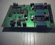
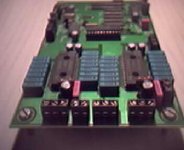
The DAC part is only shown for one channel. There are two TDA1541A's. Otherwise there is no need for so much trouble :->
(How the f. do you get those smiles in the text..).
Nothing special here, only decoupling is different for dig and analog power supplies. Also the routing on the board is separate. Check the pcb view from earlier posts.
This is my first DAC and this is only v1.0... I know that there are many views, from other capacitors to other (oversampling) DAC's.
I don't want to start yet another discussion here. I posted this to show the FIFO and I2S splitting, so you can use it for other designs (low clockspeeds please).
Yes, i know, it can be done in other ways with e.g. CPLD's, but i have a GAL programmer for years now and it works.
PCB was 39 euro (for 1 piece).
If it is better to do all this wayl ??? How should i know, this is only
DAC1 / version 1.0 remember...
Greetings,
Guido Baltus
The file for the GAL:
DAC
GUIDO BALTUS
CHIP GAL GAL20V8
LATCH GO WSDELAY SHIFT64 SHIFT32 DATA WS DIFFERENTIAL MUTE CLKDIV2 CLKDIV4 GND
/OE NU1 DATAL WSL I2SCLK WSR DATAR FIFOREAD CLOCK CLOCK_INV NU2 VCC
EQUATIONS
FIFOREAD = /GO +
GO * /CLKDIV2 * CLKDIV4 +
GO * CLKDIV2 * /CLKDIV4
CLOCK = CLKDIV4
CLOCK_INV = /CLKDIV4
I2SCLK = /CLKDIV4
WSL := /WS
WSR := /WS
DATAR := WS * DATA * MUTE +
/WS * SHIFT32 * DIFFERENTIAL * MUTE +
/WS * SHIFT32 * /DIFFERENTIAL * WSDELAY * MUTE +
/WS * /SHIFT32 * /DIFFERENTIAL * /WSDELAY * MUTE
DATAL := WS * SHIFT32 * MUTE +
/WS * SHIFT64 * DIFFERENTIAL * MUTE +
/WS * SHIFT64 * /DIFFERENTIAL * WSDELAY * MUTE +
/WS * /SHIFT64 * /DIFFERENTIAL * /WSDELAY * MUTE
Attachments
Marzio and others,
My idea is to allow others to order the board at the pcb manufacturer i used.
I don't have the hassle then to order a set of boards and distribute them again.
Since i have not tested all (no max yet), i am waiting a bit longer to arrange this.
I paid 39 euro's, but it should be less now since the films are made.
I think they did a good job on the board, but i cannot give anyone guaranties that it
will be ok for you. I have no relation with them and this was my first board i had
made there.
As for the 'experiments', after some testing i think it is working. That is the splitting
of the i2s signals and the fifo. I have no idea yet on sound quality etc. Maybe my routing
on the board is totally @Q#$@# so soundquality is also ...
Going to work next on powersupply and output. Many idea's on the net, so this is going to
take time.
Anyway, i am of for skiing now. So no news the coming weeks!
Greetings,
Guido
Some people asked me if it was possible to order a PCB. I found the time to put in the last component and do some testing. All seems to work. So it is possible to order one or more pcb's. Not for commercial use, but i doubt it is suited for that anyway. Hard to find even one TDA1541A S1 these days....
The pcb can be ordered at the place where i had it made. Costs are $23,95 + shipping. Orders can be made for "reorder x piece of PCB GB091202". Orders can be sent to fastpcb@olimex.com. Their website: www.olimex.com, have a look first.
I cannot tell you more than that i ordered there once and am happy with the PCB i got. But i cannot give garantees on your orders. Adjustments to the pcb are minor: some text must be scratched from some smd pads. This is easy, minor thing. Not in
the schematic: put a 1k smd resistor parallel to C8. And be carefull with the 4517, use a faster one (philips is ok). I used a MAX708 for the MAX707, works fine too.
Remember, this is not a complete DAC PCB, you still need extra powersupply, some kind of proper connection to a cd player and outputstage to get it working. I have little time at the moment and don't have this ready yet. So no comments yet on soundquality. I have a testsetup running fine (cd650/SAA7210 to the inputs, eringa geluid cd40 i/v pcb, clock back to SAA7210).
You need access to a gal-programmer to program the GAL (empty GALs do not work).
It would be nice to report back if you did go for this pcb. And i could use some suggestions for the outputstage etc.
Greetings,
Guido
P.S.
did a search here the other day and found this, so i re-invented the wheel...
Post #4
Hey gringo,we dont need no steenking dsp!!
A DSP chip is not necessary. Using one would be akin to raising Tower bridge to let a canoe through. I cite in defence of the above, the outboard dac design in the 4/96 issue of Audio
Electronics. This design, by an AD employee, using the CS8412, AD1893, SM5813 and AD1862(x2) clearly shows phase inversion being accomplished by inverting the seperate left and right
datastreams as they exit the SM5813 using a 74HC04 inverter. I have seen this done in a number of commercial and DIY schematics.
Of more interest is a Bitstream design in the september and october 1990 issues of Hifi News. In this design the inverted L/R datastream is created by feeding the normal L/R datastream to both inputs of a two input nand gate ,a 74HC132. The +L/-L and +R/-R datastreams are then created using a dual 64bit shift register (4517) and a dual 2 to 1 multiplexer (74HC157) and fed to a SAA7321 each. A 24 bit design using a CS8420 and a CS4397/43122 would need one more 4517 shift register but it would be better to use a FPGA.
All the clock generation could then be done in it and depending on the size one could go off on a tangent and implement a FIFO and/or a PLL or DLL or even a DPLL along the lines of a 74HC297 and those who think paradise is an array of dials like the one in the Krell control room in the film Forbidden Planet could decode the CD subcode and display it along with some kind of level display.
ray.
rfbrw
- Status
- This old topic is closed. If you want to reopen this topic, contact a moderator using the "Report Post" button.
- Home
- Source & Line
- Digital Source
- 2 Tda1541a