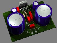
I would like to share with you my first attempt at designing a compact inverting gainclone with onboard PSU. I have read here and there on the forum and i have learned something from the more experienced of you (i hope so). So there is nothing new in my design, only i whish to learn something more and to have a compact PCB with IGC + PSU. I am open to all kind of suggestion and critcism.
Andrea
Andrea
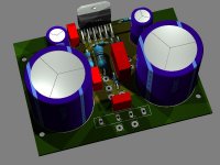
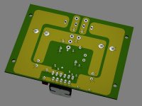
Attachments
I like the idea! C3 threw me for a minute, but I'm OK with that now. I would, however, run the ground wire for the chip directly to the ground aread instead of running it through the R2 pad. Same with the signal from the output pin to R6 instead of running it through the feedback resistor pad. Also, a bunch of people have soldered the feedback resistor directly to the chip pins, so you could even take that resistor off the board entirely if you wanted, but having a place for them on the board is nice as a backup. I would also beef up the output traces.
Overall, I like the idea and would love to know how it works when you get it implemented.
Overall, I like the idea and would love to know how it works when you get it implemented.
Nice but if you are going to make a doublesided board I'd recommend you to have a signal groundplane and let it be connected only in the Speaker ground.
It might also be a good idea to have two holes for the transformer ground. If you have a dual secondary winding you will have 4 wires also. Now you have 3 holes.
I recommend you also to decouple to ground close the LM3886. Output currents are taken from one of the rails to ground so the decoupling should be there also. Change C3 to ground and add one more on the other side.
R4 can be placed in the middle to the left of C1. No problem since you have a doublesided board.
Why don't you add 100 or 220 uF as delay for the MUTE? Then you'll have a completely silent power up.
Make the speaker traces a bit wider, 100-150 mils. No harm in that.
Have you seen my inverting Gainclone ?
P-A thanks for your hints,
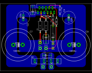
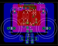
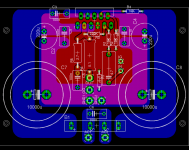
for the signal groundplane see the attached image and let me know if is good,
for the docoupling i think is better to have C3 between V+ and V- to filter differential mode noise becouse of the really high PSRR of the 3886,
for the C for the MUTE i don't use it on empirical basis: i have other chipamps with 3886 with no CM and are completely silent on power up.
ciao
andrea
Attachments
P-A i forgot to say that i see your gainclone: really really good, i like the input buffer, for the inv GC i think it's better with it, i haven't put it on my design for the sake of semplicity and becouse i use it with a pre. The only thing i can say is that the opamp used for the DC servo is too much. I think a less performing (and less expensive) opamp could be used without audible degradation.
ciao
andrea
ciao
andrea
Nice improvements. I was wondering, though, what the point of the ground wire on the bottom side of the board was now that you have a ground plane on the top side of the board? I think you can get rid of that and just have the top ground plane.
Also, be careful with your name placements to avoid getting silkscreen components over solder pads. Specifically, your output title is over your R6 pad.
Also, be careful with your name placements to avoid getting silkscreen components over solder pads. Specifically, your output title is over your R6 pad.

dfdye said:???? What good would the screw holes be for ????
I prefer to use bolt holes, I find they sound better.
")
BTW: Is there enough room for the output resistor R6? Often a 5 watter is used.
regards
Nice improvements. I was wondering, though, what the point of the ground wire on the bottom side of the board was now that you have a ground plane on the top side of the board? I think you can get rid of that and just have the top ground plane.
Also, be careful with your name placements to avoid getting silkscreen components over solder pads. Specifically, your output title is over your R6 pad.
For "ground wire on the bottom side of the board" you intend the 0 ohm resistor?
If so the answer is on the P-A reply.
The main point is to isolate power currents from signal currents.
P-A, is this the answer for dfdye question?
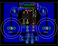
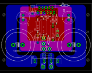
I have added screwholes, cleaned silkscreen and used a bigger package for R6,
what do you think?
Thanks to all of you.
Ciao
Andrea
Attachments
Absolutely. We are good now. I missed that you were separating the signal ground and power ground. I definitely advocate that as well! I guess I got lazy there somewhere. Sorry for the confusion!anbello said:
For "ground wire on the bottom side of the board" you intend the 0 ohm resistor?
If so the answer is on the P-A reply.
P-A, is this the answer for dfdye question?
David

I would still recommend you to have two 100 nF decoupling very close at the IC, V+ to GND and V- to GND, not only V+ to V-. This is common practice and also recommended in the datasheet.
I would possibly have V- closer the board edge in order to get some more copper to the V- pin 4.
Why R7?
Let the signal groundplane be connected at OG. Then the feedback will have it's reference there. If you of some reason want this R7 make a insulated trace directly to OG so you won't get any interference from GND1 och GND2.
Otherwise it's starting to look real good.
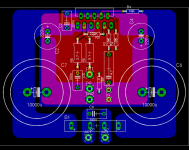
I shifted the mounting holes for Greg hint,
i addedd decoupling caps for P-A hint but fot this:
In the mean time i attach the new release.
Thanks to all
ciao
andrea
i addedd decoupling caps for P-A hint but fot this:
simply i am not able to do this in eagle (i try to substitute a wire to R7 in the back annotated sch but i don't have the wished result), i will learn to do it an then i will repost.Why R7?
Let the signal groundplane be connected at OG. Then the feedback will have it's reference there. If you of some reason want this R7 make a insulated trace directly to OG so you won't get any interference from GND1 och GND2.
In the mean time i attach the new release.
Thanks to all
ciao
andrea
Attachments
- Status
- This old topic is closed. If you want to reopen this topic, contact a moderator using the "Report Post" button.
- Home
- Amplifiers
- Chip Amps
- Inv Gain Clone with on board PSU