Dear all,
It's been a loong time ago that my analyzer was fired up last.
This, and the fact that I got named in some recent thread flames, gave me the idea that I might as well serve some experimental basis to the
discussions.. ))
))
So I assambled, as usual, several experimental bypass configurations, and measured their impedance developing across a given frequency range. Basically, I would like to compare two configurations:
The latest [according to my knowledge] "snnuberisierts" bypass arrangement a' la Carlosfm, as it is described in
in this post
The other one is the simple [classic] 10000 uF//220uF// 100nF bypass arrangement applied in the MY_ref project of Mauro Penasa.
Though I could formulate this last statement also like this: "as it was suggested by Carlosfm half a year ago."
As it can be seen from the previous, I would rather leave alone for a moment the ubiquitous "snubber" problem, that is, the reservoir caps & snubber part. About that a lot was told and measured earlier on. And, as I 've already stated, it does not have a measurable influence on the local bypass impedance [on the amplifier pins]. Which statement does not imply that it could not have an effect in other ways.
So, what I would only test & compare here is this statement of Carlos:
Let us see if I was able to reconstruct correctly:
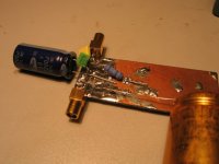
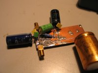
The snubber cap is 2,4nF, because it is that what I had small.
The 100 nF is the smallest possible 100V mylar cap. The resistor is
as described, 0.1W/1R. The 3,3uF I had left out for a moment.
There is a 4.700 uF reservoir cap connected, in some distance, to simulate reality.
It's been a loong time ago that my analyzer was fired up last.
This, and the fact that I got named in some recent thread flames, gave me the idea that I might as well serve some experimental basis to the
discussions..
))So I assambled, as usual, several experimental bypass configurations, and measured their impedance developing across a given frequency range. Basically, I would like to compare two configurations:
The latest [according to my knowledge] "snnuberisierts" bypass arrangement a' la Carlosfm, as it is described in
in this post
The other one is the simple [classic] 10000 uF//220uF// 100nF bypass arrangement applied in the MY_ref project of Mauro Penasa.
Though I could formulate this last statement also like this: "as it was suggested by Carlosfm half a year ago."
As it can be seen from the previous, I would rather leave alone for a moment the ubiquitous "snubber" problem, that is, the reservoir caps & snubber part. About that a lot was told and measured earlier on. And, as I 've already stated, it does not have a measurable influence on the local bypass impedance [on the amplifier pins]. Which statement does not imply that it could not have an effect in other ways.
So, what I would only test & compare here is this statement of Carlos:
Use 2200 uF +100nF (*) on the chip's Psu pins. 3,3uF (*) from V+ to V- pins. 0.1R/1W +3,3nF(*) snubber just before these caps.
(*) Use small 100V MKT caps
Let us see if I was able to reconstruct correctly:
The snubber cap is 2,4nF, because it is that what I had small.
The 100 nF is the smallest possible 100V mylar cap. The resistor is
as described, 0.1W/1R. The 3,3uF I had left out for a moment.
There is a 4.700 uF reservoir cap connected, in some distance, to simulate reality.
Attachments
Now, I would like to take a pass backwards, and show a comparison between two setup:
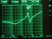
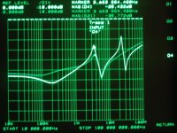
The [highlighted] Trace 1 shows : 4700uF//2200uF(local)//100nF
The dimmer Trace 2 shows: 4700uF // 100uF (local)// 100nF
The second setup is the classic. It provides a reasonably balanced and low impedance reaching up to ~2 MHz, then peaks at 3.5 MHz, then we can see the beneficial effect of the small 100nF bypass cap extending up to ~ 40-60 MHz.
As it can be seen, changing the 100uF for 2200 has lowered the ESR value below 1MHz, and has emphatised the impedance peaking at 3.5 MHz, as it was expectable. [10dB difference]
Attachments
Hey, thanks & nice to see You
So, now I would insert the "snubber"
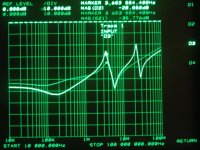
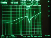
Trace 1 is highlighted & fully "snubberisiert": 4700uF // 2200uF // 100nF // .1ohm+2.4nF
Trace 2 is there for comparison, and is the classic setup.
Well, as I had suspected, we introduced some more ringing..
So, now I would insert the "snubber"
Trace 1 is highlighted & fully "snubberisiert": 4700uF // 2200uF // 100nF // .1ohm+2.4nF
Trace 2 is there for comparison, and is the classic setup.
Well, as I had suspected, we introduced some more ringing..
Attachments
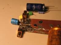
Ok, but there is one more thing to check: This was not yet the originally suggested, full setup: that one includes the 3,3uF across the floor.. that is, the supply pins.
So, I built the whole thing, two times 2200 uF //100nF, one piece of an MKT 1.5 uF /63 V across [I had this, reasonably small] and I am peeking into this assymmetrically, from the point of view of the, let's say, positive supply pin: [versus ground]
So, I built the whole thing, two times 2200 uF //100nF, one piece of an MKT 1.5 uF /63 V across [I had this, reasonably small] and I am peeking into this assymmetrically, from the point of view of the, let's say, positive supply pin: [versus ground]
Attachments
Is a snubber circuit designed for each chip or each channel? Let say I am using the calculation by Carlos and I am using the PSU for the XGC (which uses 2 chip amps per channel), do I need to have separate snubber circuits for each chip? If so, how will the calculation (capacitor values, etc) be affected?
If you look closer, it can be observed that things got a tiny bit worse.
Finally, I would like to show what have happened when I've inserted into the "classic" configuration a "passing by" noname 220 uF capacitor:
Trace 1 is : 4700uF // 220 uF // 100nF
Trace 2 is the "snubberisiert" version, without the 1,5 uF.
What I see is that not always the quantity, also the quality is important: The philips 037 series 100uF /63V small cap has had lower ESR, and provided better bypassing..
Attachments
agent.5 said:Is a snubber circuit designed for each chip or each channel? Let say I am using the calculation by Carlos and I am using the PSU for the XGC (which uses 2 chip amps per channel), do I need to have separate snubber circuits for each chip? If so, how will the calculation (capacitor values, etc) be affected?
Joseph is checking the bypass & snubber arrangement that is suggested by Carlos to be installed directly on the chips pins. Hence, what is discussed here is needed on each chip you use. There is another snubber on the PSU, which you need only once per rail.
Use 2200 uF +100nF (*) on the chip's Psu pins. 3,3uF (*) from V+ to V- pins. 0.1R/1W +3,3nF(*) snubber just before these caps.
(*) Use small 100V MKT caps
Joseph is checking the bypass & snubber arrangement that is suggested by Carlos to be installed directly on the chips pins. Hence, what is discussed here is needed on each chip you use. There is another snubber on the PSU, which you need only once per rail.
Just to clarify:
for each chip (2 per channel)
2200uf +100nf on chip's PSU pins
3.3uf from V+ to V-
and,
0.1R +3.3nf (before both chips) on each channel?
So, that's all for now. [Measurement-wise]
Some personal conclusions [though it will be partial, I would like everybody to make up their own decisions].
In the classic, 4700 [or 10000] uF // 100uF // 100nF configuration we can see that the extra added inductance originating from the reservoir cap's own ESL + stray wire inductance gets totally absorbed by the local, 220uF - 100uF bypass cap. The impedance peaking visible is due to the local resonance, between the ESL of the small 100uF local, and the 100nF local. To eliminate / dampen this resonance the usual trick is to apply a snubber cicuit. The description and effect of such a circuit is here [as tried by me]:
snubber a' la Putzeys
In that thread I also had tried to explain the difference between Zobel / snubber networks, - at least, as I see it..
What Bruno had applied, I would call that snubbing, really.
Now I would hand over to You the conversation...
And please, correct me where it is needed!
Ciao, George
Scottw,
What causes the peak? The snubber, naturally..
agent.5,
I figure the the setup suggested by carlos is 2200uF // 100nF // .1ohm+3.3nF on each chip's each supply pin, then ONE 3,3uF accross each chip.
At least this is the config that I had measured here.
Ciao, George
What causes the peak? The snubber, naturally..
agent.5,
I figure the the setup suggested by carlos is 2200uF // 100nF // .1ohm+3.3nF on each chip's each supply pin, then ONE 3,3uF accross each chip.
At least this is the config that I had measured here.
Ciao, George
Joseph K said:Scottw,
What causes the peak? The snubber, naturally..
agent.5,
I figure the the setup suggested by carlos is 2200uF // 100nF // .1ohm+3.3nF on each chip's each supply pin, then ONE 3,3uF accross each chip.
At least this is the config that I had measured here.
Ciao, George
Thanks. I am completely clueless when it comes to these snubber, zobel stuff.
Scottw,
No, not now, but have a look at this:
I tried here
Have you tried the snubbed circuit either without the 100nF bypass or with some series R (.1 to .47 ohm) on the 100nF bypass?
No, not now, but have a look at this:
I tried here
Originally posted by Joseph K
What causes the peak? The snubber, naturally..
First, thanks for posting your work.
I was trying to figure out what the snubber was reacting with that is cause the ringing; the electrolytics or the 100nF bypass, hence the suggestion about either removing the 100nF or putting some resistance in series with it.
scottw
- Status
- This old topic is closed. If you want to reopen this topic, contact a moderator using the "Report Post" button.
- Home
- Amplifiers
- Chip Amps
- "Snubber" impedance graphs