LM3886 Layout
I know this is novel here but I would suggest that you move the supply input and filter caps to one side of the 3886 and the output and output return to the other side.
This will remove any residual field from the power supply charging currents that would otherwise go across the supply ground. it would also keep the supply wires together (reducing loop area). It also flows a little better with the pinout of the device. Put the supply connections to the 3886 on opposite sides of the board to keep windows small.
-Demian
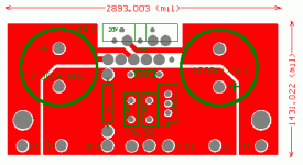
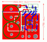
Thank you. I am according to proposing having done some modification. The boards size has reduced a lot.
the project zip file after compresses relatively big,I can't attach it ,who is interested it please give me your mail address,I 'll send the file (protel99se forms).
-digi
the project zip file after compresses relatively big,I can't attach it ,who is interested it please give me your mail address,I 'll send the file (protel99se forms).
-digi
Attachments
digi01 said:ok,i get it.
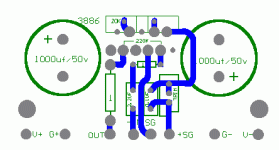
The pcb looks promising, so let's see if I can suggest some improvements. I did build that same pcb, and I can tell you what worked for me.
1) Cut off the pins you are not using from your chip before assembling it. That will let you widen the area of the V+ and V- tracks, as there shouldn't be any vestige of them on your pcb.
2) Eliminate the pads you are not using on each side. That is only pads for pins 1 and 4 should be present on the component side of your board.
3) Try to move the supply capacitors a bit so you can get similar track lengths for both, as short as possible. Make those tracks as wide as you can. You are leaving plenty of space free that should be used on V+ and V- tracks. Fill in the copper spaces.
4) Join the capacitors middle pins in the pcb to make your "dirty" ground point. In my case I use a very much older version of Traxmaker to make my pcbs, so I don't know if your program will read it to show you how. But I could do it. One thing I did was provide two small 47uF caps very close to the V+/V- pins.
5) Make some space to be used by the output resistor. Of course 1 ohm is too big, so you may try three 1 ohm / 1 watt oxide resistors in parallel there.
6) In my case I didn't use a double sided pcb for my IGC, and things were fine. A double sided board may bring some benefits for separating supply and signal tracks but not much more, though I might be wrong.
7) Make your signal tracks wider. What I always do, when I finish the tracks layout, is fill up all the copper areas. Not using a ground plane but widening the tracks already there with the fill-in tool. A side benefit for that is that you may use SMD parts if you want to. For me it makes tracks better in all respects and lowers inductance.
Carlos
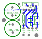
Remarkable improvement. I have a few comments and suggesstions still.
1) Double sided boards with plated through holes are much more reliable than single sided boards.
2) With a double sided board you can do some tricks to reduce the magnetic field around the high current connections, like make a stripline for the output and for the power. this means putting the power traces on one side and the ground return on the opposite side. Doing this for the area around the caps will help as well. The inductance is reduced and the capacitance is increased when you do this.
3) Bring the output and the output ground return off the board as close together as possible. I would use a pair of wires as close to the chip as possible. If you need the output damper put it in line with the cables. (I have never needed it but I have only used the amps in a closed system).
I would be reluctant to remove pins, the chances of chopping the wrong one is too high, and in the production environments i usually work in its too time consuming.
I like substantial pads on both sides of the board for any connections. Unused pins do not need pads but they do need holes (and the holes will be plated).
Input pins should have short narrow traces to reduce capacitive coupling.
The power supply is off board but you need to have the filter caps as close to the rectifier and the rectifier as close to the transformer as possible to reduce the fields from the charging. When the rectifier starts conducting it passes a large current to charge the cap. two problems- 1) large drops across the wires because of the high peak currents, 2) large magnetic fields from the currents.
I hope this helps.
-Demian
1audio said:Remarkable improvement. I have a few comments and suggesstions still.
1) Double sided boards with plated through holes are much more reliable than single sided boards.
2) With a double sided board you can do some tricks to reduce the magnetic field around the high current connections, like make a stripline for the output and for the power. this means putting the power traces on one side and the ground return on the opposite side. Doing this for the area around the caps will help as well. The inductance is reduced and the capacitance is increased when you do this.
3) Bring the output and the output ground return off the board as close together as possible. I would use a pair of wires as close to the chip as possible. If you need the output damper put it in line with the cables. (I have never needed it but I have only used the amps in a closed system).
Of course it would be better to use a double sided pcb, as you can take advantage of many aspects like those you mentioned. But it's also more expensive and very hard to DIY.
I would be reluctant to remove pins, the chances of chopping the wrong one is too high, and in the production environments i usually work in its too time consuming.
We are not talking production environments here, but DIY projects. The first GC projects proposed here not only chopped off the pins, as they also used p2p wiring. Hardly a production procedure.
I think you can use a pcb, but the unused pins should go.
I like substantial pads on both sides of the board for any connections. Unused pins do not need pads but they do need holes (and the holes will be plated).
I prefer substantial pads too, as long as they don't interfere with track's width. Unused pins need no pad and should be chopped off if they would interfere with a better pcb design. And even if you leave them I would never put pads on both sides.
Input pins should have short narrow traces to reduce capacitive coupling.
Capacitive coupling can occur if tracks are very close or if there is a ground plane on the other side. But not because the tracks are wide.
The power supply is off board but you need to have the filter caps as close to the rectifier and the rectifier as close to the transformer as possible to reduce the fields from the charging. When the rectifier starts conducting it passes a large current to charge the cap. two problems- 1) large drops across the wires because of the high peak currents, 2) large magnetic fields from the currents.
Then all projects proposed here are all wrong, because the caps are closer to the power amp chip and far from the rectifiers, relatively speaking. Maybe that's why they sound so good.
Carlos
In DIY you are free to make the projects as difficult as you like. Petr Mare demonstrated in the Lyra Connoiseur preamps that airplane P toP construction can sound better but its performance is highly variable and very difficult to build.
The wider traces make more area for capacitive coupling. Going to an input pin on an IC the impedances are very high and the sensitivity is very high. Minimizing the exposed area is a good idea. However on the negative input if tied to a low impedance can be used as a guard ring around the positive input.
The rectifier issue I brought up againg because its important. I would have external capacitors for the primary resivoirs and keep the 60Hz noise away from the amp. The loop between the diodes and the filter caps has the highest noise energy and should be kept well away from the inputs to the amp. Have people tried it both ways and confirmed which it better? Its an easy experiment to try. If you have a magnetic field proble you can see the magnitue of the energy easily.
-Demian

Hi Demian:
>In DIY you are free to make the projects as difficult as you like. Petr Mare demonstrated in the Lyra Connoiseur preamps that airplane P toP construction can sound better but its performance is highly variable and very difficult to build.<
I'd like to offer some perspective here. The Connoisseur 2.0 (designed by Petr) was built with discrete componentry and a high proportion of air-dielectric construction, and sounded exceptional for its day. Now, however, I have developed a phono stage which uses mainly opamps and no air-dielectric whatsoever, yet still manages to beat the Connoisseur 2.0 in about 75% of all sonic parameters which are musically important to me (although the 2.0 still does certain things which I find musically compelling). So you shouldn't think that air-dielectric is _essential_ for performance - it isn't. Schematic, pcb layout, operating points, componentry and other basic issues still matter a lot.
OTOH, the latest Lyra-Connoisseur 5-0 measures (and sounds) much better again than either the 2.0 or the opamp prototype. It does use air-dielectric construction, discrete componentry, and it is true that so far I have not been able to reach this level of sound without using air-dielectric construction.
At this point in time, my take is that while air-dielectric can provide worthwhile benefits, if there are lacking areas in the fundamental design, air-dielectric is not going to magically convert a sow's ear into a silk purse.
If you can devote sufficient design time for fully honing the schematic, pcb layout, operating points + componentry as well as devising an efficient and effective air-dielectric structure, you will probably have very good measured and sonic results.
But if you need to choose how to spend your time, putting more effort on the design fundamentals will lead to better results than prioritizing too much time for a cool-looking air-dielectric structure.
hth, jonathan carr
Perspective
Jonathan:
Thanks for the update on the Lyra projects. I agree with your fundamental point- that basic design issues are more important.
I'm delighted that you are getting good results from an IC based preamp, since they remove some of the most tedious steps in the fabrication of an audio circuit. And they can be much more stable over time.
-Demian

digi01 said:
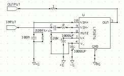
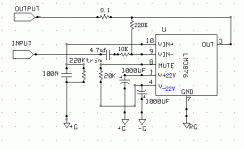
Put a capacitor from pin 8 to ground.
Carlos
- Status
- This old topic is closed. If you want to reopen this topic, contact a moderator using the "Report Post" button.
- Home
- Amplifiers
- Chip Amps
- 3886IGC protel layout share