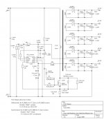
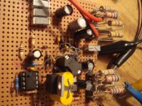
In the meantime I went on with the onboard flyback for my class D full bridge....
The flyback can deliver 3 x 16.5V fully independend isolated for low side and both floating highside drivers. Furtheron +/- 12.5V for signal conditioning circuits & protection relais etc....
The input voltage range is from 20V up to 150V. Well, start up voltage is higher and depends on the load... with 5W load it starts up at 35V, start up voltage can be reduced be reducing R_flb01 and/or increasing C_flb03.
The design offers two operation modes:
Synchronized or selfresonant.
In selfresonant mode the soft switching is perfectly nice ZVS for turn ON and OFF as well. Turn OFF ZVS is ensured by limiting dv/dt with the snubber cap. ZVS for turn ON is ensured by the resonance of the transformer inductance & snubber cap. Vds is sloping down from max value to zero (or even into freewheeling) with a sine wave function. The control IC turns the MOSFET ON when the zero crossing detection is triggered. The gate drive delay is adjusted in a way that the MOSFET turns ON be t Vds is zero.
Attachments
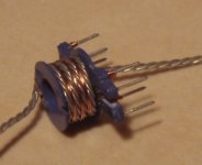
The transformer is a RM5 with N49 ferrite. The airgap is 0.15mm (manually grind  ).
).
Load regulation error of the directly regulated output voltage is below my measurement limit.
Load regualtion error of the free running 16.5V outputs is about 3% if the load is stepped from 54mA to 160mA.
The transformation ratio is designed to allow perfect resonant ZVS snubbering up to 120V input voltage.
).Load regulation error of the directly regulated output voltage is below my measurement limit.
Load regualtion error of the free running 16.5V outputs is about 3% if the load is stepped from 54mA to 160mA.
The transformation ratio is designed to allow perfect resonant ZVS snubbering up to 120V input voltage.
Attachments
Why is the snubber lossless? seems that Q1 turning on will cause the snubber cap to discharge through the snubber resistor. if the cap can fully discharge, then you still have F*C*V^2 losses on the snubber resistor. if it can't, then you still have losses because the snubber no longer allows for ZVS becuase the cap will have positive voltage across it.
that said, it will move the losses off of the FET nicely.
Have you concidered a snubber like attached:
the leakage inductance here will charge the cap through the diode. when the transistor turns on, the cap will charge the inductor through the other diode. the charged inductor will then discharge back into Vcc. only diode losses exist.
as with the slope snubber you are currently using, duty ratio should be limited to values that allow the snubber to transfer/dissipate all of stored energy in the snubber.
The snubber I have posted is deviously not lossless still, as energy transfered to the snubber results in current flowing in T1 and Q1 (and diodes). as a result, RMS currents in the circuit are higher. there is an optimal value of C that provides sufficient snubbing, while preventing excessive RMS currents.
Attachments
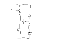
Functional description of lossless snubber
Hi theChris! (...many Chris around here? )
Have a more detailed look to the text and the schematic. There are two possible operating modes. Synchronized (from any other source) and selfresoant. Your points are only for the synchronized operating mode. And even then take care the losses in the snubber resistor are just halt of what you are stating, because only the discharge is going through R_flb_snub.
Means per cycle we loss 0.5*C*U^2. Making a power of P=f*0.5*C*U^2. 330pF would make unacceptable losses. So in this config the snubber cap is 15pF, allowing just a so so ZVS for turn OFF. With 15pF and 400kHz and 300V this means 270mW in the resistor. And also no snubbering for turn ON. The circuit can handle but is making about 0.5W more losses than in selfresonant mode.
In selfresonant mode the snubber cap is 330pF directly parallel to the MOSFET (Well in my current set up I put the cap to GND instead to the source of the MOSFET, this allows to see the freewheeling currents by watching the voltage drop across R_flb_shunt).
Function of the lossless snubber:
When the transistor is OFF the energy is transferred to the secondaries. Vds = input voltage + reflected voltage.
The reflected voltage is the output voltage times the transformation ratio. In this design it is about 130V.
At the end of the energie transfer towards the secondaries the current in the transformer is zero. The voltage across the transformer is the reflected voltage and the snubber cap is charged to Vds = input + reflected. The circuit is forming a resonant circuit with the snubber cap and the transformer inductance. The resonance frequency in my design is 817kHz. Vds is starting to slope down by this function u(t)= (input voltage + reflected voltage) - reflected voltage*cos(w*t).
The lowest voltage which this function can reach is the input voltage minus the reflected voltage. This will happen 612ns after the cos sloping has started. If the input voltage is less than the reflected voltage than the MOSFET body diode will clamp and some freewheeling time is taking place. If the input voltage is higher than the reflected voltage then no perfect ZVS is possible any more. Even if we switch the MOSFET on after 612ns, Vds will be positive and a hard switching current spike will occur.
My design is turning ON after about 600ns, the zero current detection is triggered about 300ns after the sloping is starting (this is the point where the voltage across the transformer is changing the sign).The additional required 300ns are generated by the IC internal delay + my gate turn on delay.
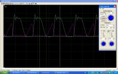
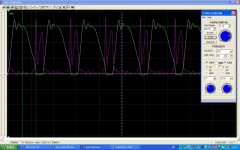
In the following I will show screen shots of the flyback with 8.7W load and different input voltages: 40V, 110V, 180V.
40V:
You can clearly see the frewheeling phase. The MosFet is being switched ON again during this time. Very nice ZVS.
White trace: Vds, 100V/grid
Red trace: Voltage drop across R_flb_shunt, 0.5V/grid ==> 278mA/grid
Hi theChris! (...many Chris around here? )
Have a more detailed look to the text and the schematic. There are two possible operating modes. Synchronized (from any other source) and selfresoant. Your points are only for the synchronized operating mode. And even then take care the losses in the snubber resistor are just halt of what you are stating, because only the discharge is going through R_flb_snub.
Means per cycle we loss 0.5*C*U^2. Making a power of P=f*0.5*C*U^2. 330pF would make unacceptable losses. So in this config the snubber cap is 15pF, allowing just a so so ZVS for turn OFF. With 15pF and 400kHz and 300V this means 270mW in the resistor. And also no snubbering for turn ON. The circuit can handle but is making about 0.5W more losses than in selfresonant mode.
In selfresonant mode the snubber cap is 330pF directly parallel to the MOSFET (Well in my current set up I put the cap to GND instead to the source of the MOSFET, this allows to see the freewheeling currents by watching the voltage drop across R_flb_shunt).
Function of the lossless snubber:
When the transistor is OFF the energy is transferred to the secondaries. Vds = input voltage + reflected voltage.
The reflected voltage is the output voltage times the transformation ratio. In this design it is about 130V.
At the end of the energie transfer towards the secondaries the current in the transformer is zero. The voltage across the transformer is the reflected voltage and the snubber cap is charged to Vds = input + reflected. The circuit is forming a resonant circuit with the snubber cap and the transformer inductance. The resonance frequency in my design is 817kHz. Vds is starting to slope down by this function u(t)= (input voltage + reflected voltage) - reflected voltage*cos(w*t).
The lowest voltage which this function can reach is the input voltage minus the reflected voltage. This will happen 612ns after the cos sloping has started. If the input voltage is less than the reflected voltage than the MOSFET body diode will clamp and some freewheeling time is taking place. If the input voltage is higher than the reflected voltage then no perfect ZVS is possible any more. Even if we switch the MOSFET on after 612ns, Vds will be positive and a hard switching current spike will occur.
My design is turning ON after about 600ns, the zero current detection is triggered about 300ns after the sloping is starting (this is the point where the voltage across the transformer is changing the sign).The additional required 300ns are generated by the IC internal delay + my gate turn on delay.
In the following I will show screen shots of the flyback with 8.7W load and different input voltages: 40V, 110V, 180V.
40V:
You can clearly see the frewheeling phase. The MosFet is being switched ON again during this time. Very nice ZVS.
White trace: Vds, 100V/grid
Red trace: Voltage drop across R_flb_shunt, 0.5V/grid ==> 278mA/grid
Attachments

110V: Vds is still sloping down to zero, but no more freewheeling. We are close to the upper end of the input voltage which results in ZVS. The MosFet is being switched ON at Vds=0. Still very nice ZVS.
FYI 110V is the intended nominal supply voltage in my class D amp (+/-55V).
White trace: Vds, 100V/grid
Red trace: Voltage drop across R_flb_shunt, 0.5V/grid ==> 278mA/grid
FYI 110V is the intended nominal supply voltage in my class D amp (+/-55V).
White trace: Vds, 100V/grid
Red trace: Voltage drop across R_flb_shunt, 0.5V/grid ==> 278mA/grid
Attachments
180V: Vds cannot slope down to zero anymore. Theoretical lowest Vds of this resonant sloping is 50V. The MosFet is being switched ON after about 600ns and hitting into about 60V-70V. Not nice anymore, but this design has quite some margin vs defects.
White trace: Vds, 100V/grid
Red trace: Voltage drop across R_flb_shunt, 0.2V/grid ==> 111mA/grid
White trace: Vds, 100V/grid
Red trace: Voltage drop across R_flb_shunt, 0.2V/grid ==> 111mA/grid
Attachments
...but of course also this topology has its disadvantages.
1.
The MosFets must have a voltage rating well above two times of the intended input voltage. For offline applictaions you would need 800V better 1000V devices. Technically no problem, but giving some headache to the financial controler of your company.
2.
The sloping times are reducing the possible duty cycles, resulting in slightly higher peak currents compared to unsubbered critical conduction mode. How much time you want to spend is depending on how fast you want to switch. Never switch faster than necessary, fast switching and high di/dt chasing through your PCB will always cause EMI issues especially in the UHF frequency range.
3.
For high power designs (say above 300W) you should generally go for continuos operating modes. Instead of discontinous or critical conduction.
...hmm... for applications, which are not in trouble with the above points - this topology should be pretty fine.
- Status
- This old topic is closed. If you want to reopen this topic, contact a moderator using the "Report Post" button.
- Home
- Amplifiers
- Power Supplies
- Lossless Snubbered Flyback