Hello,
After quite some experience with stabilisation in power supplies for B+ I noticed that regulation with zeners somehow has a negative impact on the sound. Only stabilisation on the basis of just resistors does not seem to degrade the sound. I refer to the type of stabilisation that for example Norman Koren uses in his TENA-amplifier. The link is:
http://www.normankoren.com/Audio/TENA.html
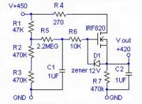
Of course this can be done with tubes. However, often a simple Mosfet follower is more easy to make and takes little extra space in existing applications. In the next figure I have included an exapmple of such a follower stabilisation. Notice that the output voltage is only stabilised relative to the input voltage. There is no absolute reference, like would occur when R2/R3 would be substituted by a zener. The so called Maida circuit with an LM317 as described in other threads is also of this kind. With resistor divider R1 and R2/R3 you can set the output voltage. R2/R3 are two resistors of 470K instead of one of 1M because a standard resistor only can take about 300V. This type of stabilisation also offers the advantage that the capacitor on the output can be small in value and therefore a good quality can easily be choosen (which then often is big in size).
This type of circuit can normally be applied without much restrictions. In a current application however I want to be sure that the B+ will not exceed 500V. As I have a choke input for B+ (with a small capacitor before the first choke) at startup for instance there can occur a short but relatively large voltage peak. My interstage is rated for 500V maximum and I don’t want it to suffer unnecessairy. So I am thinking of including a safety by adding a zener string in parallel to R2/R3 with a maximum of 475V in total (200V +200V + 75V). Normally B+ will not exceed 450V so the zeners will be out of work. When B+ will momentarilly exceed the 475V then the zenerstring will come into action. As long as the zener string is high enough above the normal operation there will be no jo-jo-ing involved (me thinks).
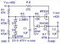
In my next post I will include the updated schematic. Also I have included an extra diode 1N4148 to protect the IRF820. The connection of the 12V zener and the 1N4148 is changed from directly on the gate to before the 10K gate resistor. I noticed that this way the circuit is more stable. But will it offer still enough protention?
Question: is this updated schematic a sound design?
Best regards, Arjen.
After quite some experience with stabilisation in power supplies for B+ I noticed that regulation with zeners somehow has a negative impact on the sound. Only stabilisation on the basis of just resistors does not seem to degrade the sound. I refer to the type of stabilisation that for example Norman Koren uses in his TENA-amplifier. The link is:
http://www.normankoren.com/Audio/TENA.html
Of course this can be done with tubes. However, often a simple Mosfet follower is more easy to make and takes little extra space in existing applications. In the next figure I have included an exapmple of such a follower stabilisation. Notice that the output voltage is only stabilised relative to the input voltage. There is no absolute reference, like would occur when R2/R3 would be substituted by a zener. The so called Maida circuit with an LM317 as described in other threads is also of this kind. With resistor divider R1 and R2/R3 you can set the output voltage. R2/R3 are two resistors of 470K instead of one of 1M because a standard resistor only can take about 300V. This type of stabilisation also offers the advantage that the capacitor on the output can be small in value and therefore a good quality can easily be choosen (which then often is big in size).
This type of circuit can normally be applied without much restrictions. In a current application however I want to be sure that the B+ will not exceed 500V. As I have a choke input for B+ (with a small capacitor before the first choke) at startup for instance there can occur a short but relatively large voltage peak. My interstage is rated for 500V maximum and I don’t want it to suffer unnecessairy. So I am thinking of including a safety by adding a zener string in parallel to R2/R3 with a maximum of 475V in total (200V +200V + 75V). Normally B+ will not exceed 450V so the zeners will be out of work. When B+ will momentarilly exceed the 475V then the zenerstring will come into action. As long as the zener string is high enough above the normal operation there will be no jo-jo-ing involved (me thinks).
In my next post I will include the updated schematic. Also I have included an extra diode 1N4148 to protect the IRF820. The connection of the 12V zener and the 1N4148 is changed from directly on the gate to before the 10K gate resistor. I noticed that this way the circuit is more stable. But will it offer still enough protention?
Question: is this updated schematic a sound design?
Best regards, Arjen.
Attachments
This circuit is also known as "Capacitance multiplier" and happens to be my favourite way of getting clean rail voltages.
By choosing the right R and C values it is possible to get a very slow startup, which is good for both tube circuits and some simple transistor amps (single rail class A stuff).
You´re absolutely right about the position of the zener diode, connecting it directly to the gate might create a transmitter rather than a regulator.
Hello Fuling, others,
Thanks for your interesting association with the capacitor multiplier. I have good experience with the capacitantce multiplier with one of my first (SS) amplifiers, the JL Hood. A reference amplifier that still would be good for 90% of all reply of music.
I have included that JLH-version of a capacitance multiplier as can be seen at various sites of Geoff and ESP. Alas, I am not that EE-educated to see the similarity between the voltage follower of my posts 1 and 2 and this original schematic. I thought it could only work as a multiplier because it has only a capacitor as reference to ground. In the follower above there is a resistive divider to ground. How will it work as a multiplier? Also R5 and C1 in the follower are merely there to filter the reference that is offered by the divider. So I must be something missing.
Could you, or anyone else, explain what is the parallel in the way it operates as a capacitance multiplier?
Best regards, Arjen.
Attachments
What you're doing in both cases is using the pass device to buffer the signal at the output of an RC low-pass filter, i.e., the voltage across the cap. The feedback in this case is merely the source/emitter follower operation of the pass device, but that feedback is the reduction of current demand on the cap. That's equivalent to multiplying the value of the cap if the pass device/buffer weren't there.
Hello Sajti, SY, others,
SY, your explanation is clear as always. Intuitively I see what you mean and to understand it fully in your EE-terms I will need some reflection.
Could someone respond to my initial question of post 1:
is the updated schematic to protection against excessive voltage with a zener string ok?
Best regards, Arjen.
Hello Tom, others,
Thanks for the suggestion. I added the diode because I saw it in several power amplifier designs with Mosfets. Now I will change the diode with a second zener of say 12V in that same opposite direction. This way, and together with the first zener, the Mosfet gate would be protected against positive and negative voltages.
I am glad with all your suggestions as the design gets more consistent.
Sajti, you wrote: 'My only note is to reduce R6 to 100-470ohms'
I will change that. In several schematics I saw this initial value of 10k for gate resistor. What could have been a valid reason for someone to make it that high?
Also I would like to repeat my first question of post 1:
'is the updated schematic with the zener string in parallel with R2/R3 to protect the output voltage against incidental excessive voltage over 450V ok?
Best regards, Arjen.
av-trouvaille said:Hello Tom, others,
Thanks for the suggestion. I added the diode because I saw it in several power amplifier designs with Mosfets. Now I will change the diode with a second zener of say 12V in that same opposite direction. This way, and together with the first zener, the Mosfet gate would be protected against positive and negative voltages.
I am glad with all your suggestions as the design gets more consistent.
Sajti, you wrote: 'My only note is to reduce R6 to 100-470ohms'
I will change that. In several schematics I saw this initial value of 10k for gate resistor. What could have been a valid reason for someone to make it that high?
Also I would like to repeat my first question of post 1:
'is the updated schematic with the zener string in parallel with R2/R3 to protect the output voltage against incidental excessive voltage over 450V ok?
Best regards, Arjen.
Hi,
the zener string looks good, there will be no problem with it.
The common value of the gate resistor is about 100-470ohms range in any amplifier I know. Someone use 10-100k in this type power supply, but as I read in some design discussion, the high value kill the HF noise reduction.
Another note (maybe just my fixed idea) the 2M2 too high (for me). Any leakage current in the protection diode network will results unwanted drops at the output. In my design I used 100k+10uF filters, but two in series
sajti
Hello,
Thanks Sajti for your suggestion for more effective filtering by also taking into account possible leakage current in the protection diode network around the Mosfet.
Tom wrote: ‘you COULD make that diode a zener as well...’
I simply presumed that adding this zener instead of the diode will add to protection. The fact that one COULD also might suggest that in your view this in fact would be exagerating precaution measures. Could you, or someone else, expand on this view some more?
At the moment I see two more questions regarding the circuit.
R4 has a value of 270 ohm. I presume this is related to limiting the inrush current for the Mosfet. I would like to keep the amount of resistors as small as possible. Can someone explain what is the penalty when R4 is simply removed ?
The other question relates to R1. In the so called riple killer as mentioned at for instance the site of Triode Dick R1 is a small capacitor. The ripple killer apparently works as a kind of shunt regulator for the ripple voltage, the AC-component of the DC-supply. Would it offer an improvement to bypass R1 in the schematic of post 1 with a small capacitor?
Best regards, Arjen.
Hello,
In the schematic of post 1 R4 has a value of 270 ohm. I presume this is related to limiting the inrush current for the Mosfet. Is this correct?
I would like to keep the amount of resistors as small as possible.
Can someone explain what is the risk when R4 is simply removed ?
Best, Arjen.
In the schematic of post 1 R4 has a value of 270 ohm. I presume this is related to limiting the inrush current for the Mosfet. Is this correct?
I would like to keep the amount of resistors as small as possible.
Can someone explain what is the risk when R4 is simply removed ?
Best, Arjen.
av-trouvaille said:Hello,
In the schematic of post 1 R4 has a value of 270 ohm. I presume this is related to limiting the inrush current for the Mosfet. Is this correct?
I would like to keep the amount of resistors as small as possible.
Can someone explain what is the risk when R4 is simply removed ?
Best, Arjen.
The R4 is not for the inrush current limitation. This will reduce the dissipation of the MOSFET, and protect it against the output short circuit.
sajti
You mean "protect" the Mosfet. If you get an output short, that Mosfet will be toast despite any protection diodes, resistors, or what-have-you. This is the voice of sad experience.
Mosfets are cheap. Get three times as many as you need because you'll lose a few during development.
Mosfets are cheap. Get three times as many as you need because you'll lose a few during development.
Hello Sajti, SY, others,
When I understand your replies correct then I can as well leave out the resistor as in my case the Mosfet will have a very modest job that will not cause it to transpire: 20 mA at a voltage difference of some 25V on average. Above all the Mosfet is on a heatsink.
Best regards, Arjen.
When I understand your replies correct then I can as well leave out the resistor as in my case the Mosfet will have a very modest job that will not cause it to transpire: 20 mA at a voltage difference of some 25V on average. Above all the Mosfet is on a heatsink.
Best regards, Arjen.
Hello,
I wonder what happens if R1 in the upper part of the voltage devider for the reference voltage will be bypassed with a small capacitor of say 0,1 uF. With only R1 the DC voltage is set. A small capacitor in parallel with R1 will also allow higher frequencies of AC to pass to ground (via the R/C-filter). So it might make to stabilisation work of the mosfet lighter because it has less high frequency ripple to cope with. The mosfet could concentrate on stabilising DC better.
So would it offer an improvement to bypass R1 in the schematic of post 1 with a small capacitor? Or is this a non-sense reasoning and does it degrade the working of the follower for some reason?
Can you comment please?
Best regards, Arjen.
Hello,
Can someone comment on this question please?
I wonder what happens if R1 of the schematics below in the upper part of the voltage divider is bypassed with a small capacitor of say 0,1 uF.
With R1 the DC voltage is set. I think a small capacitor in parallel with R1 will also allow higher frequencies of AC to pass to ground (via the R/C-filter). So it might make to stabilisation work of the mosfet lighter because it has less high frequency ripple to cope with. The mosfet could concentrate on stabilising DC better.
So would it offer an improvement to bypass R1 in the schematic of post 1 with a small capacitor? Or is this a non-sense reasoning and does it degrade the working of the follower for some reason?
Best regards, Arjen.
Hello,
In my previous post I did not include the updated schematic.
Here it is.
I wonder if someone can comment on this question please.
What happens if R1 of the schematics below in the upper part of the voltage divider is bypassed with a small capacitor of say 0,1 uF.
With R1 the DC voltage is set. I think a small capacitor in parallel with R1 will also allow higher frequencies of AC to pass to ground (via the R/C-filter). So it might make to stabilisation work of the mosfet lighter because it has less high frequency ripple to cope with. The mosfet could concentrate on stabilising DC better.
So would it offer an improvement to bypass R1 in the schematic of post 1 with a small capacitor? Or is this a non-sense reasoning and does it degrade the working of the follower for some reason?
Best regards, Arjen.
Attachments
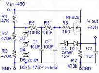
SY said:The cap will, I think, degrade line rejection. But if you put it across the Zener string, it might help at frequencies where its impedance is lower than the Zener string impedance.
Yes, it can help if connected parallel with the zener string. But I think that it's not really necessary, due the double 100k-10uF filters, which will kill all the noises coming from the zeners...
sajti
- Status
- This old topic is closed. If you want to reopen this topic, contact a moderator using the "Report Post" button.
- Home
- Amplifiers
- Tubes / Valves
- Resistive ps voltage follower