Hello All,
Here is the schematic of the power amp section of Kyocera R-861 receiver. It has MOSFETs in the driver stage. I have very little knowledge in the audio amplifier design so please excuse any of my mistakes. I believe there is an error in the schematic. The value of R520L is marked as 180ohms, but I believe it should be 2.2K to have the symmetrical open loop gain for positive and negative swings of the signal. Am I correct? If so will this kind of asymmetry have any impact on frequency response and the distortion of the amp? Should I change that value to 2.2K. Any advice is appreciated.
Thanks,
Routhun
Attachments
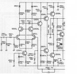
ilimzn said:No, Q508L is the wrongly marked one, it should be 180 ohms, instead of 2.2k.
Q508L is a transistor.
I think if you work out the collector currents, assuming Q505 and Q506 have the same currents, you probably will find that the Vb-to supply of the drivers is different and that the different resistor still gives the same current. But that's from just a quick look.
Jan Didden
routhun said:Thanks ilimzn!
Hi Janneman,
I can understand Ilimzn is referring to R519L instead of Q508L.
So my question is should I replace R519L with 180ohms? Will it make any difference in sound?
Routhun
I don't know if make a difference in sound but surely it make difference in good working of circuit (which actually, if the R519 value is real and not only - as i think - a print mistake on schematic, is severely unbalanced).
Ciao and merry xmas to all!
")
Piercarlo
routhun said:Thanks ilimzn!
Hi Janneman,
I can understand Ilimzn is referring to R519L instead of Q508L.
So my question is should I replace R519L with 180ohms? Will it make any difference in sound?
Routhun
G'day.
Yes, R519L, the emitter resistor of Q508L, should be changed from 2k2 to 180R to balance the currents. However, the designers might have done this as an after thought for a reason. Note that one of the frequency compensation capacitors (C505L) connects to the collector of Q508L. I'm guessing that perhaps the amplifier wasn't stable with the VAS currents balanced, so the gain of amplifier stage formed my Q508L was reduced by increasing the emitter resistor.
Cheers,
Glen
G.Kleinschmidt said:
Note that one of the frequency compensation capacitors (C505L) connects to the collector of Q508L. I'm guessing that perhaps the amplifier wasn't stable with the VAS currents balanced, so the gain of amplifier stage formed my Q508L was reduced by increasing the emitter resistor.
Cheers,
Glen
Compensation capacitor C 505 compensate open loop gain for *all* VAS circuitry, and not only for Q508. You must see the output network of VAS (apart from VBE multiplier and following output stage) as a parallel of C505, R521 and R522. This pole is rawly settled for a minimun frequency of 21 KHz (in the reality more high due to other "hidden" conductance connected in parallel to ouput: collector output conductance, loading impedance from output stage and so on - this compensation is also aided by a second pole on the differential input stage output which "kill" it's voltage gain above 240 kHz - rawly).
A raw estimation for the real roll-off of this pole may be just a doubled frequency, which let to intend two thing: this amplifier is intended for achieving very high slew rates, extended power bandwidth with light and splitted compensation and relying heavily for it's stability on the "hard" separation operated from the MOS driver between the VAS load and any kind of output load reflected on VAS itself. Is a very sofisticated design and, for somewhat, enough critical to discouraging "lighthearty" intervention. Open loop gain (about 90 dB) is high but prudently limited by local emitter degenerations.
Hi!
Piercarlo
When the amplifier is at equilibrium (no signal), voltages across R517 and R518 have to be nearly identical, so voltages referenced to corresponding power supply rail at emitters of Q509 and Q509 have to be nearly identical too. With resistor R519 being about 12 times the value of R520, Q509 should draw 12 times more current than Q508. R519 is uncorrectly labelled, it should 180 Ohm. Check the real circuit, it is probably only the schematics which is wrong.
Piercarlo said:
Compensation capacitor C 505 compensate open loop gain for *all* VAS circuitry, and not only for Q508.
Yes, I can see that, but since it connects to the collector of Q508, if the designer(s) felt the need to tweak the open loop gain to solve stability issues, they may have gone to the emitter resistor of Q505 as well.
This is just a postulation, of course. It's probably just a drafting error. However if it isn't, I'd suppose the designer(s) could have had a good reason for doing it, and err on the safe side before fixing it. The circuit would be heavily unbalanced with the 2k2 resistor, and it would certainly seem odd to lower the open loop gain in such a way, but I've seen worse compromises made to solve stability issues.
G.Kleinschmidt said:
Yes, I can see that, but since it connects to the collector of Q508, if the designer(s) felt the need to tweak the open loop gain to solve stability issues, they may have gone to the emitter resistor of Q505 as well.
This is just a postulation, of course. It's probably just a drafting error. However if it isn't, I'd suppose the designer(s) could have had a good reason for doing it, and err on the safe side before fixing it. The circuit would be heavily unbalanced with the 2k2 resistor, and it would certainly seem odd to lower the open loop gain in such a way, but I've seen worse compromises made to solve stability issues.
Stability issues of this circuit may be effectively solved only redefining the entire chain of gains that contributes to the overall gain of the VAS. Deactivating one side of the VAS may just reduce the overall gain of a factor of two, imho insufficient to cope with unstabilities if they occurs - which, in turn, desimmetrize the working of circuit not only from the gain point of view but also from the slew-rate point of view, i.e. just the key feature of this circuit. If the symmetrical SR is not guaranteed, then is most valuable to come back to a standard asymmetrical VAS stage, less critical e more reliable of this, which, by itself, need some care not only in the choice of components (Mosfets are the most critical because more difficult to "complementarize" than bipolars) but also in the design of phisical PCB layout.
Hi - Merry Xmas to all!
Piercarlo
Piercarlo said:
, imho insufficient to cope with unstabilities if they occurs"
Well that would depend entirely on the margin of instability. Supposing the resistor value was intentional (ie, not simply a drafting error), I simply gave a possible reason for it's strange value. Like I said previously, I've seen stranger compromises made to solve last minute stability issues; after all, an amplifier can hardly be put onto the market if it oscillates. If you have a better theory I'd like to hear it.
G.Kleinschmidt said:
Like I said previously, I've seen stranger compromises made to solve last minute stability issues; after all, an amplifier can hardly be put onto the market if it oscillates. If you have a better theory I'd like to hear it.
The theory of "last minute strange compromises" may be a good one. My elucubrations was made in the hipothesis of a quiet, savvy revision of the design. If you are right... then I may only discourage any buying of amplifiers (as of any others equipments) from this firm. First of all because a "last minute strange compromise" as this, plainly reported on schematics, don't allow further trusting on team design ability to cope safely with circuital problems!
. An inspection of fisical construction for detecting "last minute" PHYSICAL correction is recommended! Happy Xmas... despite of "last minute" odds!
Piercarlo
Trust me, the resistor needs to be 180 ohms... the amp is similar to the Kyocera A700 I had and I know the topology.Besides, think about it: there is a 12-fold difference in degeneration of the top and bottom side, as well as, potentially a >12-fold difference in maximum current sourced. Compared to that, compensation would be WAY down on the list of things to look at.
ilimzn said:
Obviously ilimzn is right .
The resistor MUST be 180 Ohms!
Hi All,
Last night I had a chance to open the cover of this receiver, and verified that error is only in the schematic actual circuit has 180 ohms resistor in place of R519L. Thanks for all the valuable posts, we can learn a good deal of information from them. Let us put an end to this discussion here.
Hi Zeon,
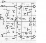
Here is the actual values for transistor types.
Routhun
Last night I had a chance to open the cover of this receiver, and verified that error is only in the schematic actual circuit has 180 ohms resistor in place of R519L. Thanks for all the valuable posts, we can learn a good deal of information from them. Let us put an end to this discussion here.
Hi Zeon,
Here is the actual values for transistor types.
Routhun
Attachments
Tube_Dude said:
Obviously ilimzn is right .
The resistor MUST be 180 Ohms!
routhun said:Hi All,
Last night I had a chance to open the cover of this receiver, and verified that error is only in the schematic actual circuit has 180 ohms resistor in place of R519L.
Tube Dude, hopefully that clears it up.
- Status
- This old topic is closed. If you want to reopen this topic, contact a moderator using the "Report Post" button.
- Home
- Amplifiers
- Solid State
- Error in power amplifier schematic