Hi all,
I am working on an amplifier (how suprising") but I haven't decided wich
but I haven't decided wich
emitter follower structure to use. It will be a class A 10 W amplifier whith
symmetric design. Not a big deal at all and to be honest I do not like the
amount of NFB it will use, but I could not figure out how to decrease the
output resistance without strong NFB. (As I remember there was a thread
called "I would like to see your amp" or something like this, where HH
described sortly his amplifier and according those lines it is damn close to
what I imagine as a really good amplifier. (Just local NFB, DC coupled,
completly FET based...) But there is a secret about the output resistance
and damping factor wich I do not know yet.)
Anyway, the reason because I wrote that I need some help regarding this
complex emitter follower I found in JLH's amplifier design book. I wasn't
seelpingThe first BJP is a simple emitter follower I understand this. The DC offset
between its base and emitter is around 0.6 Volts or so and I can bias the
output by implementing a proper voltage across the 0.22 resistor. So the
bias would be lets say for 1A*0.22Ohms + 0.6 V = 820 mVolts. But what is the
function of the other transistor? In the book it was meantioned as an
alternate and superior version of the simple darlington structure, so I
assume the first transistor would take over the task of a first BJT in the
commercional darlington leaving the real work - providing the dissipation
for the 1A - to the second one. But how does this 1 Amp divide up between
the two transistors? The first transistor has a resistor between the power
supply and its colletor providing some voltage wich is - I think - definitly
0.6 Volts or so beacuse of the base-emitter drop voltage of the second
transistor, wich is paralell with this resistor. Also in the book both the
emitter and the collector resistance had the same 100 Ohms value. In this
way there should flow about 6mA (0.6/100) across the first BJT leaving 994
mA to the second BT. (Assuming that the emitter and collector current is
equal.)
to much last night beacuse I was wondering how this can work at
all, how does it the trick JLH meantioWhat I do not understand is:
This topology is implemented in many applications as the final stage wich
drives the speaker, so the whole signal voltage is apparent at the base of
both BJTs. I just can not see how could then the second BJT work with the
whole signal without any emitter voltage potential. (Emitter connected
directly to the power rail.) As I see it should cut one half of the signal.
Or the second BJT is not an emitter follower? Maybe they are grounded
emitters using each other as an active load? Anyway is it not class B? And
at least JLH meantioned that this type of topology provides less output
imedance as a simple emitter follower. (According to the book the output
impedance of the complex emitter follower equals the output impedance of a
simple emitter follower devided by the Hfe of the second BT.) Why and how?
So, please somebody tell me the working mechanism of this follower
structure...
Thanks anyway and sorry for the long mail.
bt

I am working on an amplifier (how suprising
but I haven't decided wichemitter follower structure to use. It will be a class A 10 W amplifier whith
symmetric design. Not a big deal at all and to be honest I do not like the
amount of NFB it will use, but I could not figure out how to decrease the
output resistance without strong NFB. (As I remember there was a thread
called "I would like to see your amp" or something like this, where HH
described sortly his amplifier and according those lines it is damn close to
what I imagine as a really good amplifier. (Just local NFB, DC coupled,
completly FET based...) But there is a secret about the output resistance
and damping factor wich I do not know yet.)
Anyway, the reason because I wrote that I need some help regarding this
complex emitter follower I found in JLH's amplifier design book. I wasn't
seelpingThe first BJP is a simple emitter follower I understand this. The DC offset
between its base and emitter is around 0.6 Volts or so and I can bias the
output by implementing a proper voltage across the 0.22 resistor. So the
bias would be lets say for 1A*0.22Ohms + 0.6 V = 820 mVolts. But what is the
function of the other transistor? In the book it was meantioned as an
alternate and superior version of the simple darlington structure, so I
assume the first transistor would take over the task of a first BJT in the
commercional darlington leaving the real work - providing the dissipation
for the 1A - to the second one. But how does this 1 Amp divide up between
the two transistors? The first transistor has a resistor between the power
supply and its colletor providing some voltage wich is - I think - definitly
0.6 Volts or so beacuse of the base-emitter drop voltage of the second
transistor, wich is paralell with this resistor. Also in the book both the
emitter and the collector resistance had the same 100 Ohms value. In this
way there should flow about 6mA (0.6/100) across the first BJT leaving 994
mA to the second BT. (Assuming that the emitter and collector current is
equal.)
to much last night beacuse I was wondering how this can work at
all, how does it the trick JLH meantioWhat I do not understand is:
This topology is implemented in many applications as the final stage wich
drives the speaker, so the whole signal voltage is apparent at the base of
both BJTs. I just can not see how could then the second BJT work with the
whole signal without any emitter voltage potential. (Emitter connected
directly to the power rail.) As I see it should cut one half of the signal.
Or the second BJT is not an emitter follower? Maybe they are grounded
emitters using each other as an active load? Anyway is it not class B? And
at least JLH meantioned that this type of topology provides less output
imedance as a simple emitter follower. (According to the book the output
impedance of the complex emitter follower equals the output impedance of a
simple emitter follower devided by the Hfe of the second BT.) Why and how?
So, please somebody tell me the working mechanism of this follower
structure...
Thanks anyway and sorry for the long mail.
bt
Attachments
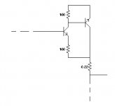
The first transistor can be thought of as an error-amplifier. It responds to the potential difference between its base and emitter terminals.
You can think of the second transistor as a common-emitter stage, providing lots of gain.
So, you have an error amplifier, and a gain stage. A complete system employing negative feedback! Using only 4 components!
It works like this: Suppose you raise the input potential a bit... The first transistor will see an increased VBE, and will respond to this by increasing its collector-current. This collector-current will flow through the base-emitter junction of the second transistor - it also responds by increasing its collector-current.
Here's the clever bit: This increased collector current will raise the potential of the output of your circuit. However, if it raises it too much, what happens to the VBE of the first transistor?
That's right, the VBE seen by the first transistor shrinks, it stops passing current, the second transistor also stops passing current, and your output voltage will fall!
Of course, it won't fall far, because the first transistor will switch on again and cause the voltage to stabilise. In reality, you won't observe any "hunting", but I think it helps understanding if you break everything down and think in this simplistic way...
So, the circuit uses 100% negative feedback to achieve a gain of 1, a high input impedance, and low output impedance. It's neat
Cheers,
Mark
Hmmm.... Thanks for the explanation mhennessy . I always have some problem when thinking about NFB circuits beacuse they are a bit unreal for me. (Modifying a signal wich have already passed through the network by coupling it back to the input...Somewhat not logical, even if all the elements are ultra fast in the circuit. If I try to imagine how such amplifiers work always some kind of oscillation falls into my mind and in the next minute I am completly confused about the whole theory. Anyway, it seems that I can not avoid using NFB and your post was a great help.
aka Sziklai pair or Complementary Feedback Pair (CFP)
I think the second transistor is suposed to be a pnp?
http://jever.phys.ualberta.ca/~gingrich/phys395/notes/node97.html#ch5DarlSzik
I think the second transistor is suposed to be a pnp?
http://jever.phys.ualberta.ca/~gingrich/phys395/notes/node97.html#ch5DarlSzik
CFP
The circuit you show is a so called "complementary follower pair". It has a voltage gain of 1 (as emitter follower) and there is an additional current gain created by 2nd transistor (PNP). The circuit has strong local NFB, very good linearity and is better than Darlington pair. To see an example of amps with this circuit you might click on the www button below this message.
The circuit you show is a so called "complementary follower pair". It has a voltage gain of 1 (as emitter follower) and there is an additional current gain created by 2nd transistor (PNP). The circuit has strong local NFB, very good linearity and is better than Darlington pair. To see an example of amps with this circuit you might click on the www button below this message.
Re: CFP
There seems to be a lot of controversy regarding the "best" BJT output stage. Prof. Leach discounts this approach and considers the Darlington, overall, to be superior. He claims that the use of local negative feedback can cause oscillations in the output stage and that the bandwidth is reduced vs. what a Darlington would provide due the Miller effect causing the junction capacitance to be much larger. I belive the Darlington also provides the lowest output impedance.
I think the complementary follower does have better linearity due to the local feedback, but Leach appears to think the price of this is too high. Regardless, some good amps have been built using both approaches, so it may be worth some more investigation.
PMA said:The circuit you show is a so called "complementary follower pair". It has a voltage gain of 1 (as emitter follower) and there is an additional current gain created by 2nd transistor (PNP). The circuit has strong local NFB, very good linearity and is better than Darlington pair. To see an example of amps with this circuit you might click on the www button below this message.
There seems to be a lot of controversy regarding the "best" BJT output stage. Prof. Leach discounts this approach and considers the Darlington, overall, to be superior. He claims that the use of local negative feedback can cause oscillations in the output stage and that the bandwidth is reduced vs. what a Darlington would provide due the Miller effect causing the junction capacitance to be much larger. I belive the Darlington also provides the lowest output impedance.
I think the complementary follower does have better linearity due to the local feedback, but Leach appears to think the price of this is too high. Regardless, some good amps have been built using both approaches, so it may be worth some more investigation.
CFP stability
to Jeff R:
yes, the question is whether we speak about DIY approach without instruments or about a try to find optimal solution. With oscilloscope and simulated speaker load it is easily possible to make the CFP circuit stable. I also use capacitive load up to 10uF. Modern BJT devices, as 2SA1943 and 2SC5200 are superb in linearity and fast enough to enable application of frequency correction by a small cap. The amp (I speak about push-pull follower from my web page) is very very quick, no SR or fh limitation, several hundreds of kHz even with freq. compensation. I have tried, measured and listened both approachs and I do prefer CFP. Another big advantage is much better thermal stability, as there is only one Vbe.
Note: please take to the account that a frequency stability of Darlington is not any better than CFP
Yes, the thermal stability issue is good news - you only need to monitor the temperature of the drivers, so the VBE-multiplier transistor can be mounted on the much smaller driver heatsinks. No need to put it on the main heatsink with all the layout issues that go with it.
One problem with the CFP - you have to control the bias voltage much more accurately than you do with EF output. This is a reason to use the EF - you might get a slightly worse result, but it will be more consistent with time and temperature.
As a lot of you will know, Doug Self has lots of good information about this...
BTW, Banfi T. - you won't be able to avoid feedback in transistor circuits. Even the humble EF has 100% negative feedback
I agree unequivocally with Professor Marshall Leach.
I have built two otherwise identical SS amplifiers, one with a CFP (Sziklai) output stage, the other with a conventional double emitter follower, a Self Type III.
The comparison is very obvious audibly, the only way that counts.
The problem appears to be oscillation in the CFP, particularly the negative rail block. This oscillation robs detail, and creates spurious intermodulation products which destroy any musicality. We can fix this by simply strapping a 100pF cap from base to collector of the driver, however. But then if you listen, the musical presentation lacks vitality, sounds 'drained'.
Leach is quite right; the price of securing stability with the CFP is so high sonically you might as well use an emitter follower, where Zout is actually not so low, but the sonics are far superior.
Go back to the Type III Self double emitter follower, and the vitality is immediately apparent. There is no comparison audibly. Vocalists no longer sound 'tired'.
Of course, to a technologist, the emitter follower lacks the appeal of the CFP, which just reeks of elegance, but sounds like !@#$.
Furthermore, the much touted advantage of superior thermal stability is overshadowed by very tetchy and low bias voltage requirements; it must be deadly accurately set, since with only two pn junctions across the bases of the drivers there is little room for error; the Vbe of a large transistor varies considerably with collector current and the tolerance setting bias is far less sensitive.
Another major problem the CFP has is the switch off behaviour; as the output comes off, the driver has difficulty with the extremely fine control of collector/emitter voltage because of the huge voltage gain of the output device, and this fudges the crossover event subliminally with spurious, short term oscillation whichever remedy you use to prevent it. This might make them suitable for Class A, but for Class AB, no dice.......
Sorry, long post......
Cheers,
Hugh
www.aksaonline.com
CFP x double EF
Mhennessy, AKSA - thank you for very valuable replies. We may have different experience with different circuits - that might be a source of little bit different point of view.
BTW - I do not admire Leach amp that much. How about Halcro dm58?
Anyway, thanks once more for valuable replies.
Mhennessy, AKSA - thank you for very valuable replies. We may have different experience with different circuits - that might be a source of little bit different point of view.
BTW - I do not admire Leach amp that much. How about Halcro dm58?
Anyway, thanks once more for valuable replies.
Re: CFP x double EF
Yikes! For some of us, that is heresay!
As an engineer with tin ears myself, I am in total awe of Leach's amp, and have been since I was an EE student in 1976 when I, by pure chance, happened to read his article in Audio. That article changed everything for me. I don't know what you don't like about the design, but from a theoritical standpoint, it has all the ingredients for a top-of-the-line amplifier. I think that futher work could be done on it to get more incremental improvements (i.e. split power supplies, driving the voltage gain stages from a different supply than the current amplifiers, buffering of the second voltage gain stage from the diff amp stage, etc.) and using better components and possibly hardwiring the electronics vs. printed wirting boards, but the basic elements are there.
I have considered using the basic design but changing things so it will work at a lower voltage so as to turn it in to a Class A amplifier. I think that would be slick, though I am not all that convinced that a Class A amplifiers should really sound any better than a properly biased AB amplifier, all other things being equal.
Still, it is fun to try to different things and it would be nice if, someday, we can learned what it really takes to create the "ultimate amplifier".
PMA said:
BTW - I do not admire Leach amp that much.
Yikes! For some of us, that is heresay!
As an engineer with tin ears myself, I am in total awe of Leach's amp, and have been since I was an EE student in 1976 when I, by pure chance, happened to read his article in Audio. That article changed everything for me. I don't know what you don't like about the design, but from a theoritical standpoint, it has all the ingredients for a top-of-the-line amplifier. I think that futher work could be done on it to get more incremental improvements (i.e. split power supplies, driving the voltage gain stages from a different supply than the current amplifiers, buffering of the second voltage gain stage from the diff amp stage, etc.) and using better components and possibly hardwiring the electronics vs. printed wirting boards, but the basic elements are there.
I have considered using the basic design but changing things so it will work at a lower voltage so as to turn it in to a Class A amplifier. I think that would be slick, though I am not all that convinced that a Class A amplifiers should really sound any better than a properly biased AB amplifier, all other things being equal.
Still, it is fun to try to different things and it would be nice if, someday, we can learned what it really takes to create the "ultimate amplifier".
Hi PMA,
It's a pleasure! But I should confess that it has been a while since I've had a chance to do some solid practical work with output stages. I've read a lot and learned a great deal from this forum, and Doug Self's book (amongst others) in the last few years, and I'm looking forward to starting my monoblock projects in the new year...
I currently favour the CFP, but I am in a very fortunate position: I have salvaged 4 identical chassis that used to be 24V PSU's in a large mixing desk
These are the perfect shape and size for monoblocks, and I've already got quite a lot of the planning done. I will build 4 identical units, but will experiment with different configurations. I reckon that the front-end will be standard stuff, but I will try both EF and CFP output stages. Having 4 units will let me do proper AB testing, as I can have two different pairs in the listening room at any time...
More details to follow
AKSA said:
Another major problem the CFP has is the switch off behaviour; as the output comes off, the driver has difficulty with the extremely fine control of collector/emitter voltage because of the huge voltage gain of the output device, and this fudges the crossover event subliminally with spurious, short term oscillation whichever remedy you use to prevent it.
Hugh,
for my part, I actually love your long posts. I still have to go back to the thread about VAS stages and write down my thoughts there.
I think I have gathered by now you don't like Miller caps. Actually, they have a double linearizing effect: first of all, they swamp the voltage dependent BC junction capacitance. For example, a Miller capacitance that can be 2 to 15 pF depending on the drive level will be paralled with something like 100 pF that does not change with the drive. Secondly, it provides local current feedback, lowering the output impedance of the stage and again making it more linear. Whatever the reason for the "drained sound", it was not the Miller as such (which you didn't say) but probably something like too much bandwidth lost.
Regarding the passage quoted above, I wonder if there aren't ways of curing the CFP. The first approach would be to use emitter degeneration resistors on the output devices. Then there was something that was used a lot by Elektor. The output was divided down by a low impedance (maybe 30 R) divider and fed back to the bases or emitters (will have to look at the articles again) of the drivers. This gave some "global local" feedback over the positive and negative side of the circuit. Also, it was possible to set a gain >1 for this stage. I played with the circuit years ago (using IRF5490/9540 as well as those Toshiba complementary IGBTs everybody was crazy about for a while). It was very stable but there was a spike driving a triangle into low impedance I couldn't get rid of. Might be a good idea to repeat that experiment with a few Sanken bipolars.
Regards,
Eric
Comples etc
Hi BanFi,
I know the feeling. For me it helps if I realise that the NFB circuit actually needs an input signal different from the feedback signal to function. We often assume that the feedback signal cancels the input signal, but that is not true!. Just looking at AC for simplicity, in the circuit you propose, there will always be an "error voltage" which is a small AC signal difference between the base and the emitter of the input transistor. This signal is amplified with the open loop (without feedback) gain, so really it is a "normal" amplifier. This is the same with opamps. An opamp with 100% feedback (noninverting follower) is assumed to have + and - inputs that are the same. This is not so. If the opamp has an open loop gain of say 100k, then at 1V out there will be a minuscule 10uV inpout signal between the 2 inputs. Small, but necessary: without it there would be no output signal.
Am I making sense?
Jan Didden
Banfi T. said:Hmmm.... Thanks for the explanation mhennessy . I always have some problem when thinking about NFB circuits beacuse they are a bit unreal for me. (Modifying a signal wich have already passed through the network by coupling it back to the input...Somewhat not logical, even if all the elements are ultra fast in the circuit. If I try to imagine how such amplifiers work always some kind of oscillation falls into my mind and in the next minute I am completly confused about the whole theory. Anyway, it seems that I can not avoid using NFB and your post was a great help.
Hi BanFi,
I know the feeling. For me it helps if I realise that the NFB circuit actually needs an input signal different from the feedback signal to function. We often assume that the feedback signal cancels the input signal, but that is not true!. Just looking at AC for simplicity, in the circuit you propose, there will always be an "error voltage" which is a small AC signal difference between the base and the emitter of the input transistor. This signal is amplified with the open loop (without feedback) gain, so really it is a "normal" amplifier. This is the same with opamps. An opamp with 100% feedback (noninverting follower) is assumed to have + and - inputs that are the same. This is not so. If the opamp has an open loop gain of say 100k, then at 1V out there will be a minuscule 10uV inpout signal between the 2 inputs. Small, but necessary: without it there would be no output signal.
Am I making sense?
Jan Didden
Well, I'm online...
So, thanks everybody helping me...
janneman:
Maybe it will suprise some of you after what I questioned, but I'm an EE. So I learned the usual staff, and in theory I know how NFB works, but since as far no one could tell me exatly what is going on in an amplifier wich uses a strong global feedback loaded with a real speaker (including crossover network), nor I could figure out some details I'm a bit afraid of taking things easy and thinking like: this is a stage with great gain and we should utilize a feedback and it will be OK. (Just as if we were talking about OPAMPS.)
For example in this case after what I learned in this forum I would state the following question: (one out of many)
- The second BJT is a grounded emitter, wich has a lot of gain. Its emitter resistance (or impedance) is about 26mV / Ie assuming 25 celsius. (1A Ie means 0.0026 Ohms in theory). So, producing high gain the collector impedance must be very high. But how much? How can I calculate it. (The same question applies to every stage wich uses a current source as active load.)
In theory a current source or a symmetrical stage would mean infinite load and thus infinite open loop gain, wich is not the case. ( I mean "in theory" here the state where I am now.) At least I never saw any book in wich the open loop gain were calculated, (Including JLH's book.) But for me it would be very important, beacuse without knowing this I can just handle the situation if I think of the whole network as an OPAMP, and what I have to calculate is the feedback network. I fear with this knowledge it is better to use OPAMPS.
So please, do not misunderstood me, I am very graetful to everybody who is sharing knowledge in this forum. Maybe I'm just a stupid beginner asking trivial things...
Eric,
I do have a very good experience with CFP output stage operated in a class A. The THD measurements show the result (without global NFB!) and listening tests are very successful, no problem mentioned by Hugh.
I also had encountered some stability problems in the beginning, but it was solved by B-C caps in the drivers and - especially - a return lead from the speaker terminal! It must be unconditionally connected to the 0V point on the power supply board, not on the amp board. Connecting return lead to amp board made amp to oscillate (for large output voltage swing) at some 30 MHz! Now the circuit is perfectly stable even with a capacitive load up to several uF.
Pavel
Pavel,
You raise the interesting issue of CFP stability in Class A.
I agree with you unreservedly. Some years ago I designed a Class A SE amp, the Glass Harmony, which uses a 6SL7 front end for voltage amplification, and a SE mosfet output stage for current amplification. This is a wonderful amplifier, sounds rich, satisfying, very powerful sounding for just 28W, but just slightly more efficiency than a Baldwin Steam Locomotive.......
The output device is a pair of p type mosfets, an IRFP9140, and the bipolar driver is an 2N5551 in CFP (or more correctly, a Sziklai, a name you will doubtless recognise as Hungarian!! . ).
There are no stability issues with any kind of load, even a 6" nail, but I admit earthing is critical.
So, to revise my earlier post slightly; CFPs are dynamite in Class AB, but quite OK in Class A. Use them freely for great performance, particularly a bipolar driving a mosfet. Works great!
Cheers,
Hugh
You raise the interesting issue of CFP stability in Class A.
I agree with you unreservedly. Some years ago I designed a Class A SE amp, the Glass Harmony, which uses a 6SL7 front end for voltage amplification, and a SE mosfet output stage for current amplification. This is a wonderful amplifier, sounds rich, satisfying, very powerful sounding for just 28W, but just slightly more efficiency than a Baldwin Steam Locomotive.......
The output device is a pair of p type mosfets, an IRFP9140, and the bipolar driver is an 2N5551 in CFP (or more correctly, a Sziklai, a name you will doubtless recognise as Hungarian!! .
).There are no stability issues with any kind of load, even a 6" nail, but I admit earthing is critical.
So, to revise my earlier post slightly; CFPs are dynamite in Class AB, but quite OK in Class A. Use them freely for great performance, particularly a bipolar driving a mosfet. Works great!
Cheers,
Hugh
AKSA wrote:
Thats exactly what I intend to do but in the version with gain >1 as mentioned by capslock.
The two nice things about it are a) you can drive the output very close to the rails and b) you can use low Vceo drivers.
Regards
Charles
Use them freely for great performance, particularly a bipolar driving a mosfet.
Thats exactly what I intend to do but in the version with gain >1 as mentioned by capslock.
The two nice things about it are a) you can drive the output very close to the rails and b) you can use low Vceo drivers.
Regards
Charles
- Status
- This old topic is closed. If you want to reopen this topic, contact a moderator using the "Report Post" button.
- Home
- Amplifiers
- Solid State
- Complex Emitter follower