I agree that the datasheet is a bit obfuscated, but these ICs are not so hard to use. I got IR2112 working in my first attempt, I only blew one of these ICs and it was because I shorted the logic supply to ground (strange way to blow it).
Could you describe the exact problems or doubts that you have ran into?
Could you describe the exact problems or doubts that you have ran into?
Hi,
Try testing it in simulation too. It'll allow you to work out at least a few particulars in a much faster, and cheaper way.
Also, when you're stuck, it allows you to post a schematic for us which we really appreciate when it comes to helping to troubleshoot.
IR seems to have a Pspice model for that driver.
The ir2110 4 my class d power amp
I have attached my schmatic 4 the power amp. My problem I dont get any output, why i connect on the board. am getting a very small single which look like noise. Simulation dont give me result also. could you plz advice me
cheers
I have attached my schmatic 4 the power amp. My problem I dont get any output, why i connect on the board. am getting a very small single which look like noise. Simulation dont give me result also. could you plz advice me
cheers
Attachments
Yep good eye, V3 is the wrong way around ")
In general, to me it looks like your housekeeping and rail voltages are a complete mess. Reread the data sheet, try looking at the schematic of the chip on it and that should help you decipher things.
VCC is scary wrong. Use a seperate supply for VCC, reference it off Vss properly. VDD could likely be built off it, properly bypassed, but it may require another supply too, whatever the rest of your logic circuitry is using. Not sure about that. Eva?
You're missing a connection node for Vcom.
Forget Rd and the "snubbers". They're the last thing you ought to be worrying about at this point.
Reference your input signals properly as already mentioned in the above post... and that should do the trick.
There is actually nothing wrong with V3, as it's drawn backwards but the voltage is negative to compensate.
The chip is not wired properly, and if you tried it that way in a real prototype it's very likely to be damaged thus requiring replacement. Be careful since that kind of electronic toys are not cheap
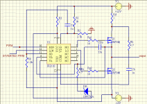
VCC(+) and COM are the supply pins for the lower quasi-floating gate drive cell.
VB(+) and VS are the supply pins for the higher floating gate drive cell.
VDD(+) and VSS are the supply pins for the (quite fragile) logic input stage, which may be fed from a lower voltage such as 5V, or directly from VCC.
The ground of the fully floating gate drive cell (VS) is allowed to rise up to 500V above the ground of the lower cell (COM), and is also allowed to fall as much as 15V below COM for short periods of time.
The ground of the logic input stage (VSS) is allowed to float almost +/-5V with respect to COM in order to allow for better noise rejection in very complex applications. That feature is hardly required so COM and VSS are usually tied together.
The following schematic shows a working IR2112 application (a weaker version of IR2110) driving two banks of three IGBTs, with external buffers and connected as a half bridge. By 'working' I mean that I'm listening to it right now.
The supply voltage for the lower cell is 18V and is derived through R17 and D10 in a very straightforward way. The supply voltage for the logic section is 5V and is derived from those 18V through a L78L05 as I'm using also TTL gates and optocouplers. The supply voltage for the upper cell is derived from the 18V of the lower cell through D3, so that C7 gets replenished every time the lower cell turns on. The capacitor values shown are high enough to prevent any trouble due to starvation.
HIN and LIN turn on the corresponding high and low gate drive cells when they are driven logic-high. SD disables the entire IC if it's driven logic-high, and it does in such a way that the gate drive cells won't be turned on again until the next rising edge of the corresponding HIN or LIN input (thus allowing to terminate switching cycles prematurely and leaving both cells off until the next cycle begins).
IR2112 is rated at +-200mA so it requires buffering in most applications, but IR2110 is rated at +-2A and can drive gates directly, altough the "resistor+resistor/diode" networks shown are strongly recommended in order to control switching slopes and EMI.
The 2.2uF capacitors shown are high ESR in order to allow for paralleling 100nF ceramics without any resonance (checked in the actual PCB) and the resulting capacitor pairs are placed in close proximity.
The chip is not wired properly, and if you tried it that way in a real prototype it's very likely to be damaged thus requiring replacement. Be careful since that kind of electronic toys are not cheap
VCC(+) and COM are the supply pins for the lower quasi-floating gate drive cell.
VB(+) and VS are the supply pins for the higher floating gate drive cell.
VDD(+) and VSS are the supply pins for the (quite fragile) logic input stage, which may be fed from a lower voltage such as 5V, or directly from VCC.
The ground of the fully floating gate drive cell (VS) is allowed to rise up to 500V above the ground of the lower cell (COM), and is also allowed to fall as much as 15V below COM for short periods of time.
The ground of the logic input stage (VSS) is allowed to float almost +/-5V with respect to COM in order to allow for better noise rejection in very complex applications. That feature is hardly required so COM and VSS are usually tied together.
The following schematic shows a working IR2112 application (a weaker version of IR2110) driving two banks of three IGBTs, with external buffers and connected as a half bridge. By 'working' I mean that I'm listening to it right now.
An externally hosted image should be here but it was not working when we last tested it.
The supply voltage for the lower cell is 18V and is derived through R17 and D10 in a very straightforward way. The supply voltage for the logic section is 5V and is derived from those 18V through a L78L05 as I'm using also TTL gates and optocouplers. The supply voltage for the upper cell is derived from the 18V of the lower cell through D3, so that C7 gets replenished every time the lower cell turns on. The capacitor values shown are high enough to prevent any trouble due to starvation.
HIN and LIN turn on the corresponding high and low gate drive cells when they are driven logic-high. SD disables the entire IC if it's driven logic-high, and it does in such a way that the gate drive cells won't be turned on again until the next rising edge of the corresponding HIN or LIN input (thus allowing to terminate switching cycles prematurely and leaving both cells off until the next cycle begins).
IR2112 is rated at +-200mA so it requires buffering in most applications, but IR2110 is rated at +-2A and can drive gates directly, altough the "resistor+resistor/diode" networks shown are strongly recommended in order to control switching slopes and EMI.
The 2.2uF capacitors shown are high ESR in order to allow for paralleling 100nF ceramics without any resonance (checked in the actual PCB) and the resulting capacitor pairs are placed in close proximity.
??Eva: wrote:The 2.2uF capacitors shown are high ESR in order to allow...
sivan_and said:
Without the high ESR you'd need to use other means to damp the Q of the resonant circuit that would form by bypassing it with another cap.
Pafi:
It's all a matter of choosing the proper IGBT, see mine:
They seem likely to get well together in groups
Tim:
Current tail length is shown as "tf" in the previous figure. I definitely can live with a 24ns tail of no more than 2A. Also, MOSFET devices show similar tails in practice because the internal resistance and inductance of the gate cell structure prevents the charge from being removed uniformly, and some parts of the die just continue conducting longer than others (usually the lower the Rds-on, the longer the current tail because lower Rds-on dies require more cells and are more complex).
Concerning the XOR splitter with dead time, you will have to figure out the schematic, but it's very straightforward. It's main feature is uniform propagation delays.
It's all a matter of choosing the proper IGBT, see mine:
An externally hosted image should be here but it was not working when we last tested it.
They seem likely to get well together in groups
Tim:
Current tail length is shown as "tf" in the previous figure. I definitely can live with a 24ns tail of no more than 2A. Also, MOSFET devices show similar tails in practice because the internal resistance and inductance of the gate cell structure prevents the charge from being removed uniformly, and some parts of the die just continue conducting longer than others (usually the lower the Rds-on, the longer the current tail because lower Rds-on dies require more cells and are more complex).
Concerning the XOR splitter with dead time, you will have to figure out the schematic, but it's very straightforward. It's main feature is uniform propagation delays.
Why do you think this? Don't you know up-to-date IGBTs? They have been designed especially for high freq class D! (OK, not especially for audio.) They have advantages and disadvantages too. (Low conduction loss, low Qrr...) At high voltage IGBT is the most cost-efficient solution. And quality depends on controlling.
(OK, not especially for audio.) They have advantages and disadvantages too. (Low conduction loss, low Qrr...) At high voltage IGBT is the most cost-efficient solution. And quality depends on controlling.Pafi said:It seems to be optimized especially for paralelling! What type is it? Will you test if they can bear 2...3 times of a single device capability?
Try to figure out first
I've already used a pair of them in a PFC front-end conducting up to 20A total during input rectified sine peaks, and there were no traces of hot spotting despite the two IGBTs being quite spaced in the heatsink.
Tekko:
The key is in actual device parameters. If you research further into the topic, you may discover that there are much more types of IGBTs other than the good old ones used to drive three-phase motors below 1Khz. You may also discover that MOSFETs actually suck for high voltage class D due to their clumsy and slow body diode, which becomes even worse for lower Rds-on devices. On the other hand, IGBTs don't have a body diode, so they require an external one that may be Hyperfast, SiC or whatever you like. Furthermore, there are also IGBTs with a built-in high performance diode, which come very handy to overcome space constraints.
On the other hand, most of these high voltage MOSFETs will just *explode* as soon as load current reaches 8A or 10A if you ever try to use them in a class D output stage with a 300V or 400V supply in the same way as people uses 100V devices in small amplifiers (which feature fast body diodes). Consider the body diode from the good old IRFP460
There are special high voltage MOSFETs with fast body diodes, but their Rds-on is two or three times higher than in standard devices (and the price increases by a even higher factor).So long life to the high voltage switching bipolar transistor and its insulated-gate cousin.
So long life to the high voltage switching bipolar transistor and its insulated-gate cousin.
Blaaaaaaasphemy!!!!!!!!!!
How 'bout those nice APT or whatever mosfets?
The body diode issue in mosfets does seem to force certain topologies /babysitting circuitry though.
I'm not sure it's restrictive otherwise?
I note your nice use of the buffers after the gate driver as well, you'll find most here dont' do that, when they probably should.
Regards,
Chris
How 'bout those nice APT or whatever mosfets?
Buy if you can! I can't.
- Status
- This old topic is closed. If you want to reopen this topic, contact a moderator using the "Report Post" button.
- Home
- Amplifiers
- Class D
- The Ir2110