Hi Charles,
I want to use the Clocked version of Class-D amp in Single Supply mode. But my confusion is regarding feedback network, i want to use feedback from before filter and to inverting input of comparator. there is no level shifting though. So what would be a good scheme to connect the feedback, is it possible or not.
Reply soon.
Sincere regards,
kanwar
Attachments
ThanX Charles
SALUTE Charles,
ThanX for the Help.
Can we Swap the inputs of IR2110 instead , I mean to say Hi and Lo inputs swapping. is it possible. If not , than would I have to add another opamp as summing integerator for this, is there will be an DC offset Problem asscociated with single supply feedback.
kindly advise us.
No, we dont want to cook Voice- Coil, I simply want to use these 2 modules in Bridging topology , there is no cooking indeed.
Sincere Regards,
kanwar
phase_accurate said:NFB from before the filter is usually done with a summing integrator. Since these are "inverting" you'd have to swap the inputs of your comparator.
But for heaven's sake ,what do you want to use this for (i.e. single supply) ? As a voice-coil cooker ?
Regards
Charles
SALUTE Charles,
ThanX for the Help.
Can we Swap the inputs of IR2110 instead , I mean to say Hi and Lo inputs swapping. is it possible. If not , than would I have to add another opamp as summing integerator for this, is there will be an DC offset Problem asscociated with single supply feedback.
kindly advise us.
No, we dont want to cook Voice- Coil, I simply want to use these 2 modules in Bridging topology , there is no cooking indeed.
Sincere Regards,
kanwar
You can of course change phase by swapping the input control signals.
Between the lines I somehow feel that you wanted to use the comparator as integrator to avoid another op-amp. You definitely can't do this for several reasons.
So you will definitely need another op-amp for the integrator. There would also be a possibility for doing this just passively. But apart from simplicity I don't see any advantages of doing so.
There is no offset problem if everything is properly referenced to the same "ground", which is not the negative supply rail but an "artificial" at half the supply voltage.
Regards
Charles
phase_accurate said:You can of course change phase by swapping the input control signals.
Between the lines I somehow feel that you wanted to use the comparator as integrator to avoid another op-amp. You definitely can't do this for several reasons.
So you will definitely need another op-amp for the integrator. There would also be a possibility for doing this just passively. But apart from simplicity I don't see any advantages of doing so.
There is no offset problem if everything is properly referenced to the same "ground", which is not the negative supply rail but an "artificial" at half the supply voltage.
Regards
Charles
Hi Charles ,
ThanX for your Advise,
So what will be your suggesstion:
1) using an extra opamp
or
2) Swapping the control inputs.
We want to use control signal swapping as these can contribute lot more to simplicity.
Advise us, so that we can move further.
Regards,
kanwar
Hi Kanwar
You seem to be a multiple personality !
I am afraid you don't have a choice of either one or the other. You'd have to do both. You will have to use a summing integrator for your feedback (alternatively you can use the same integrator for both NFB and triangle generation).
And you will have to change the phase of the PWM signal by either:
1.) swapping the comparator inputs or
2.) swapping the fixed H and L signals on the 2nd XOR inputs or
3.) swapping the mosfet driver's control inputs.
Regards
Charles
You seem to be a multiple personality !
So what will be your suggesstion:
1) using an extra opamp
or
2) Swapping the control inputs.
I am afraid you don't have a choice of either one or the other. You'd have to do both. You will have to use a summing integrator for your feedback (alternatively you can use the same integrator for both NFB and triangle generation).
And you will have to change the phase of the PWM signal by either:
1.) swapping the comparator inputs or
2.) swapping the fixed H and L signals on the 2nd XOR inputs or
3.) swapping the mosfet driver's control inputs.
Regards
Charles
Still Confusing
hi Charles nice advise , but still under confusion.
I want to use a carrier based Class-D approach.
therefore , I will take LM6172 as Triangle generator.
According to my understanding about what you have said is that the triangle generator can be used as both for feedback and integerator, Am I right if not then correct me. than what about comparator.
regards,
kanwar
The circuit as shown would not work. You would need a summing integrator. You could do this to a ceratin degree by connecting a capacitor from the inverting input of the comparator to signal ground. But this would be suboptimal.
If you use the opamp as triangle generator directly then you can't use it as integrator as well at the same time (though I have to do some thinking about that) but you could use an opamp as a self-oscillating class-d modulator directly (i.e. hysteresis modulator).
If you want to generate the triangle by integrating a rectangular, then you can use the integrator for the NFB as well at the same time (like the old Sony patent).
But you will definitely need to add something to your schematic !
Regards
Charles
passive intergrator v.s. op amp:which will produce less distortion?
the passive one produces a slightly non-linear triangle,but the nonlinear effects is very low when the level of triangle is small.
(maybe the harmonics involved can be analysised by taylor series expansion,but i haven't do any calculations yet.)
Some peple reports that a hyersis modulator made of 555 timer,with a hyersis of VCC/3,produces only 0.8%(maybe 2.5%) THD.
op amp has finite SR and it's sensitive to noise and TIM.
fast op amp can prevent this,but they are also expensive.
phase_accurate said:So you will definitely need another op-amp for the integrator. There would also be a possibility for doing this just passively. But apart from simplicity I don't see any advantages of doing so.
is there any gate drive ICs with internal dead-time?
tawen_mei said:I think you will have a shoot-thru problem.
The two drivers in 2110 are independent, so they may overlap, and there's nothing in your circuit that creates dead-time.
tawen_mei said:I think you will have a shoot-thru problem.
The two drivers in 2110 are independent, so they may overlap, and there's nothing in your circuit that creates dead-time.
They're being driven by a pair of gates which are splitting the signal, so the drive signals won't overlap.
The dead time is created internally by the driver's turn on prop. delay Vs turn off prop delay, this is all that IR uses in their reference design.
Dead time is a bad thing! (may the flames begin)
Has anyone tried one of those predictive gate drivers yet?
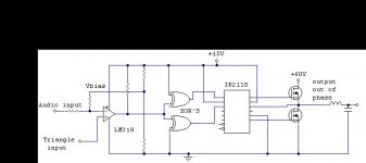
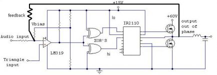
mmmm, workhorse, your design resembles a lot to what I posted in this forum about 1 year ago or more (LM6172 triangle generator, XOR gates at IR2110 input, LM319 comparator...
I did some experimentation and also with symmetric supplies and no level shift, with all (triangle gen, error opamp and comparator) using a single supply referenced to Vss, with of course capacitive coupling at the input, but had variable offset problems and distortion figures were not very good so I abandoned that approach although it was much simpler.
If that's an experiment and you are doing it to learn and for personal use, no problem for me (that's what this forum was created for).
Have luck.
classd4sure said:
They're being driven by a pair of gates which are splitting the signal, so the drive signals won't overlap.
The dead time is created internally by the driver's turn on prop. delay Vs turn off prop delay, this is all that IR uses in their reference design.
Dead time is a bad thing! (may the flames begin)
Has anyone tried one of those predictive gate drivers yet?
I thought the IR211x had some built-in dead time.
My impression is that dead time is bad, though it may be better to margin toward DT than toward cross conduction in most cases these days. But, DT does raise distortion and noise, so I can understand your interest in adaptive DT. I appreciate how you have shed light upon the problems concerning MOSFET body diode conduction, too.subwo1 said:
I thought the IR211x had some built-in dead time.
Why thank you. I appreciate that you're one of the guys who brought it to my attention.
It seems clear both overlap and lots of dead time aren't the answer and so the middle ground must be found. Predictive delay is said to "eliminate" body diode conduction! I'm not that picky, adaptive would do fine for now, and the effort would have big payoffs, aside from THD and EMI, you gain a very robust gate drive that has an iron grip on any mosfet you want to swap in your circuit.. we don't drive our cars blind, why do it with mosfets?
The benefits of doing it adaptively are many. Drawback is complexity (DIY'rs don't seem to care about cost). Lot's of IC drivers have used it for awhile (late 80's?)..they seem geared towards low voltage regulators, and I really hate being a slave to an IC, (I have some ideas..) but for now the LM5401 seems rather quick, with nicely matched, short delays and good for 100V, with a full bridge that's respectable. It has a single input, so if you start off opposite phased split signals that can't overlap, a full bridge should be easy.
Everyone seems to like using the IR2XXX stuff, but the delays and matching are horrible, sure it's good to 600V, but I haven't seen that put to use either?
Hopefully they'll realise there's a market for better drivers for something other than notebook, PDA and cell phones!
classd4sure said:
Why thank you. I appreciate that you're one of the guys who brought it to my attention.
It seems clear both overlap and lots of dead time aren't the answer and so the middle ground must be found. Predictive delay is said to "eliminate" body diode conduction! I'm not that picky, adaptive would do fine for now, and the effort would have big payoffs, aside from THD and EMI, you gain a very robust gate drive that has an iron grip on any mosfet you want to swap in your circuit.. we don't drive our cars blind, why do it with mosfets?
The benefits of doing it adaptively are many. Drawback is complexity (DIY'rs don't seem to care about cost). Lot's of IC drivers have used it for awhile (late 80's?)..they seem geared towards low voltage regulators, and I really hate being a slave to an IC, (I have some ideas..) but for now the LM5401 seems rather quick, with nicely matched, short delays and good for 100V, with a full bridge that's respectable. It has a single input, so if you start off opposite phased split signals that can't overlap, a full bridge should be easy.
Everyone seems to like using the IR2XXX stuff, but the delays and matching are horrible, sure it's good to 600V, but I haven't seen that put to use either?
Hopefully they'll realise there's a market for better drivers for something other than notebook, PDA and cell phones!
Thanks, too. The LM5401 may not be a bad option. I may try some.
Since I mainly play around with power
supplies, I am actually quite attached to the IR211x,
though. I like the pin layout because it enables me to easily keep the
driver sections close to the MOSFETs. I have gotten its bootstrapped supply up to about 500v already. Another time, I blew one because I forgot to connect the common to the upper MOSFET source, or some such mistake, and the bootstrap supply floated up to oblivion.
I'm probably not the average DIYer since I do tend to seek value. I still spend a lot on parts, nonetheless. I think it is that I like
circuits that use easily available parts, and not too many of them as well. I often seek a compromise in design which may cost a little more but also make a design smaller or more forgiving.
I would be afraid concerning newly developed ICs that they will only be
available in surface mount. The only surface mount items I tolerate are the S0-8 MOSFETs. I may be able to avoid them, even, on the project I am working on now if switching times can be slower and gentler with small die MOSFETs.
Hi,
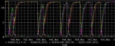
Here's a fine example of the regenerative affect acting to snap on the high side mosfets, you can also see the loading of the discrete driver.
Sadly it seems to function best as a driver when heavily loaded, I've found that a very fine balance must be achieved, because it doesn't seem possible to have non overlapping signals unless the driver is partly loaded down. This causes gate signal amplitude to vary with duty cycle. It would likely therefore be wise to select a higher drive voltage, like 15V, to lessen the detrimental affects of the gate drive signals and help maintain a constant RDSon.
To reduce the risk of overlap, it is easier to use very low current to switch the drivers with, however, too low a current and it wont' switch fast enough. This is additional to the dimensioning of the driver values to create loading as well (you need both a lightly loaded driver, and weak signals), both techniques serve to reduce overlap of the gate signals. So it is obviously only an optimal driver in terms of reduced part count, and can be made to function, although, not very well, and not without risk.
The reason to have slow turn on is to give the slow body diodes time to recover and become blocking before turning on the opposing mosfet into it.
This seems to be a half solution. Slowing of the turn on signal increases dissipation in the mosfet, and I believe helps to increase THD as well. Futhermore, it seems the regenerative affect operating on the high side mosfet's gate works against the solution.
I view all the above as strong arguments for the case of adaptive delay.
The attached gate drive signals are from simulation of a full bridge done using seperate high side Vdc sources. You can see that as loaded as it is, there's still a worrysome amount of overlap, requiring lowered current from the comparator output, but as I said that is a compromise in switching performance.
In conclusion, simple discrete drivers suck.
Thanks
Attachments
Looks almost identical to a small signal transistor common emitter circuit with about a 10K ohm pull-up on the collector. I used such as inputs to the IR211x a while back. I even had such a waveform as the output of the ubiquitous two transistor multivibrator directly feeding the input gates of the 211x, providing a drive waveform with built-in dead time for an unregulated off-line AC to DC converter.
You can also obtain such a waveform from the output of the 6n137 optocoupler, but the usefulness of it is limited by the fact that when the opto is off, the output is high. For that reason, it tends to destroy MOSFETs unless current is supplied to the emitter diodes of the optos before power is applied to the MOSFETs. The open-collector outputs of the optos need to be pulled low first.
You can also obtain such a waveform from the output of the 6n137 optocoupler, but the usefulness of it is limited by the fact that when the opto is off, the output is high. For that reason, it tends to destroy MOSFETs unless current is supplied to the emitter diodes of the optos before power is applied to the MOSFETs. The open-collector outputs of the optos need to be pulled low first.
- Status
- This old topic is closed. If you want to reopen this topic, contact a moderator using the "Report Post" button.
- Home
- Amplifiers
- Class D
- Charles, we need your help on feedback in single supply Class-D