hi luKe,
indeed the klimax uses tda7293's (3 of them), just like the quekky pi7293 , a diy triple tda7293 based amp. Basically a Klimax Klone...
It's all in the K...
indeed the klimax uses tda7293's (3 of them), just like the quekky pi7293 , a diy triple tda7293 based amp. Basically a Klimax Klone...
It's all in the K...
If you look, to the picture on page 8 of the klimax twin manual, you will see several differences between the Klimax and quekky's amp.
First of all, the Klimax obviously does not use the slave configuration, mostly because of the reduced slew rate incurred by this mode (difficulty to drive the input capacitance of the MOSFET output stage): all people I know who have listened to a single TDA7293 and a configuration of Three ICs in the slave mode configuration say the single TDA sounds best.
In fact, it looks like a Klimax twin channel is made of three TDA7293, each one with its individual servo, with an op amp based input buffer (with its own servo). I can post my guess of a schematic, or maybe we open a new thread on the subject ("Linn Klimax backengineered"?)
I bought a Linn MAJIK about ten years ago -- with the SNEAKY modules for my Kelidh's -- here's a look at the insides:
An externally hosted image should be here but it was not working when we last tested it.
An externally hosted image should be here but it was not working when we last tested it.
Some measurements of the Klimax:
http://www.soundstagemagazine.com/measurements/linn_klimax_twin/
There's a recent Linn Klimax Chakra 500 twin.
And the top Klimax 500 Solo (with Sanken transistors), sounds very good indeed, I've heard it.
Switching PSUs to a good effect.
http://www.soundstagemagazine.com/measurements/linn_klimax_twin/
There's a recent Linn Klimax Chakra 500 twin.
And the top Klimax 500 Solo (with Sanken transistors), sounds very good indeed, I've heard it.
Switching PSUs to a good effect.
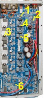
OK, let's give it a try (I won't try the SMPS, because from experience, I know it is a mess to fix) . See the pictures attached
First of all, "1" looks like a balanced to single ended conversion chip, followed by a switch, and obviously this arrangement has been kept on the new Chakra design.
"6" is a bunch of low voltage regulators (for the logic + the buffer?…) + probably a small microcontroller used to monitor the thing.
For the rest, you can see two identical amplifier section, one for each channel.
For each section, there are three TDA7293s all used with the same components. The elco is the bootstrap capacitor, there are also two large SMD caps for IC decoupling, and two small chips close to pin 1 which could be mute transistors used to protect the TDA when switching on/off the input buffer power supply (I thought first that they were used to switch the mute/stdby pin, but then they would rather have been placed on the other side of the TDA). You can see the three 0,1 Ohm epoxy coated wirewound ballast resistors in section "4".
In "4" you also see two ICs, with identical accompanying resistors/caps. In section "5" is another IC, with a different configuration. I first thought that the three Ics, perfectly aligned with the TDAs, were servos (one for each TDA). I now believe that the 2 Ics of section "4" are double op amps used for 1 servo for each of the three TDA + one servo for the section "5" IC, which then would likely be an input buffer. The servos for the TDAs ensure a good current matching between the Ics, reduce the noise and avoid elcos in the signal path. The input buffer gives a decent high output impedance and drives the bipolar inputs of the TDA (relatively high input current + high voltage offset). I'd guess IC "5" is an OPA604, AD797 or alike (FET input, low noise, low offset, stable at unity gain- don't forget that the Linn has 28,6dB total gain, and that the TDA already needs at least 26dB of closed loop gain for stability, this gives little remaining gain for the buffer stage, except if there are some dividers somewhere in the circuit).
Questions I have:
-are the TDAs are used in inverting or non inverting configuration? (my guess: not inverted)
-same question for the input buffer (although I would guess it is inverting because the input impedance of the amp is low: 7,8 k!)
-is the TDA based gain stage included in the input op amp closed loop or not (if yes the combination creates a high performance high power op amp, but you have to be careful with stability)? Personnally, this is the one I would try!
-what is section 2? Another buffer (overkill!)? Or a signal detector used to switch automatically on/off the thing (but then why these nice, expensive, blue plastic caps? And why one section for each channel?)
Has anyone any clue? Has anybody opened the little Linn Klimax box and had a look at the IC references?
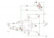
Attached in the other picture, some drawing thoughts (with a tube buffer IGC variation).
First of all, "1" looks like a balanced to single ended conversion chip, followed by a switch, and obviously this arrangement has been kept on the new Chakra design.
"6" is a bunch of low voltage regulators (for the logic + the buffer?…) + probably a small microcontroller used to monitor the thing.
For the rest, you can see two identical amplifier section, one for each channel.
For each section, there are three TDA7293s all used with the same components. The elco is the bootstrap capacitor, there are also two large SMD caps for IC decoupling, and two small chips close to pin 1 which could be mute transistors used to protect the TDA when switching on/off the input buffer power supply (I thought first that they were used to switch the mute/stdby pin, but then they would rather have been placed on the other side of the TDA). You can see the three 0,1 Ohm epoxy coated wirewound ballast resistors in section "4".
In "4" you also see two ICs, with identical accompanying resistors/caps. In section "5" is another IC, with a different configuration. I first thought that the three Ics, perfectly aligned with the TDAs, were servos (one for each TDA). I now believe that the 2 Ics of section "4" are double op amps used for 1 servo for each of the three TDA + one servo for the section "5" IC, which then would likely be an input buffer. The servos for the TDAs ensure a good current matching between the Ics, reduce the noise and avoid elcos in the signal path. The input buffer gives a decent high output impedance and drives the bipolar inputs of the TDA (relatively high input current + high voltage offset). I'd guess IC "5" is an OPA604, AD797 or alike (FET input, low noise, low offset, stable at unity gain- don't forget that the Linn has 28,6dB total gain, and that the TDA already needs at least 26dB of closed loop gain for stability, this gives little remaining gain for the buffer stage, except if there are some dividers somewhere in the circuit).
Questions I have:
-are the TDAs are used in inverting or non inverting configuration? (my guess: not inverted)
-same question for the input buffer (although I would guess it is inverting because the input impedance of the amp is low: 7,8 k!)
-is the TDA based gain stage included in the input op amp closed loop or not (if yes the combination creates a high performance high power op amp, but you have to be careful with stability)? Personnally, this is the one I would try!
-what is section 2? Another buffer (overkill!)? Or a signal detector used to switch automatically on/off the thing (but then why these nice, expensive, blue plastic caps? And why one section for each channel?)
Has anyone any clue? Has anybody opened the little Linn Klimax box and had a look at the IC references?
Attached in the other picture, some drawing thoughts (with a tube buffer IGC variation).
Attachments
if you go over to the Bridged LM4780 DIY page I started last week, we have a couple graphs of a generic bridged circuit power output and distortion -- it's National Semi which should do the boasting.
http://www.diyaudio.com/forums/showthread.php?s=&threadid=51125&highlight=
I was pleased with the initial results of the amp, but when someone suggested that I could do even better by rerouting the power supply connections I was surprised that the distortion artifacts from line interference -- 60, 120, 180 and 240 Hz -- were enough to be visible on a spectrum analyzer. You can see them if you set the analyzer center frequency at 1kHz, and set the frequency span 960 or 480 Hz.
btw, a Klimax costs around $9900, a bridged LM4780, PCB and all high quality components (ex the power transformer) cost around $20 !
You can make a quiet, high power switching supply as Linn has done, but you're not going to do it easily with a TL494 or SG3525 or SG3524.
TDA7293 with TIPxx Power Transistors
It's been nearly 6 years since the last post on this thread. I'm hoping everyone is still connected to this thread.
That's an interesting design from borgard with the TDA7293 driving a couple of BJTs to boost its output power. I think he mislabeled one of the output transistors. The NPN transistor should probably be a TIP35C and not a TIP37C. I don't think TIP37C is a valid part number, and the TIP35C is the complement to the TIP36C PNP transistor.
Is this really what Linn did? Has anyone tried this particular circuit out? If this works as shown, I'm wondering if it's possible to simplify it further by getting rid of the TL071 op-amp circuit? Any reason for that low-pass filter in the feedback loop? The original ST datasheet does not show this in the circuit. It's hard to see the + input capacitor in your drawing, but I think that's a 0.47uF, right? Any opinions about this?
I see that the feedback decoupling capacitor, C2 in the datasheet, was omitted. That's certainly easy enough to include.
I'm looking for a very cheap power amp that I can use in various projects, and this looks like a winner if it works as expected. The cost of these semiconductor parts is crazy low, and I like the idea of using discrete transistors to boost power as opposed to slaving the TDA7293s. You get more bang for the buck plus the PCB artwork is a lot easier.
Please let me know how this worked for you and if you've experimented any with it.
thanks
Hi,
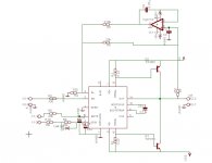
I think there is an error in the schematic post13.
R6, the upper feedback resistor, connects to the top of R7.
Should R6 connect to the bottom of R7?
The amp is DC coupled.
The opamp is a DCservo to minimise output offset.
This opamp signal needs filtering to allow audio to pass through the main amp unaffected and for VLF & DC signals to be processed.
- Status
- This old topic is closed. If you want to reopen this topic, contact a moderator using the "Report Post" button.
- Home
- Amplifiers
- Chip Amps
- About Linn power amps...