Hi,
Friends of Pass´isch I/V conversion! I have finally finished fine-tuning of my modified Pass D1 output stage. Fore interested guys here are the results…
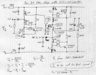
D:\Witte privat\Schaltpläne\D1 with CCS_r.JPG
To remember, that is the schematic. Nothing new, just additional CCS (imported from the Aleph P1.7) and the 2SK389 in stead of the IRF610. The only open issue was: which current gives the best sound for the 2sk389.
Well, it´s really amazing how strong the sound changes with the bias current through this FET. To make it short, I see the truth between 4,5 and 5mA. 4,5mA sounds a bit like OPA AD797 = warm, not to full, no aggression at all, extreme depth, good focus and dynamic, but not the best in class. At 5mA the story grooves more like the OPA627 or so = high focus and dynamic, more frontal than deep, harder, more precision – but close to a bit of "technical" sound. BUT: it really sounds so much better than any OPA! Exactly the difference like solid state versus Pass. Well, I´ve chosen the middle, 4,75mA. My lower BC550B has 0,61V U_be, so R2 became 128Ohms. R1 to be calculated accordingly.
BTW, my shown stage is fired by 4 x PCM1704. BB SRC4192 + DSP based four times oversampling + filtering with maximum impulse correct filter settings. Parallel voltage regulators fed from massive PSU, and so on… The sound is just incredible, no more words! Mr. Pass (and Heyink/Germany for the digital DAC stuff) fulfilled my last dream, after Amp and Pre just an appropriate DAC-output stage was missing. Done…
Regards
Klaus
Friends of Pass´isch I/V conversion! I have finally finished fine-tuning of my modified Pass D1 output stage. Fore interested guys here are the results…
D:\Witte privat\Schaltpläne\D1 with CCS_r.JPG
To remember, that is the schematic. Nothing new, just additional CCS (imported from the Aleph P1.7) and the 2SK389 in stead of the IRF610. The only open issue was: which current gives the best sound for the 2sk389.
Well, it´s really amazing how strong the sound changes with the bias current through this FET. To make it short, I see the truth between 4,5 and 5mA. 4,5mA sounds a bit like OPA AD797 = warm, not to full, no aggression at all, extreme depth, good focus and dynamic, but not the best in class. At 5mA the story grooves more like the OPA627 or so = high focus and dynamic, more frontal than deep, harder, more precision – but close to a bit of "technical" sound. BUT: it really sounds so much better than any OPA! Exactly the difference like solid state versus Pass. Well, I´ve chosen the middle, 4,75mA. My lower BC550B has 0,61V U_be, so R2 became 128Ohms. R1 to be calculated accordingly.
BTW, my shown stage is fired by 4 x PCM1704. BB SRC4192 + DSP based four times oversampling + filtering with maximum impulse correct filter settings. Parallel voltage regulators fed from massive PSU, and so on… The sound is just incredible, no more words! Mr. Pass (and Heyink/Germany for the digital DAC stuff) fulfilled my last dream, after Amp and Pre just an appropriate DAC-output stage was missing. Done…
Regards
Klaus
Attachments
That's fine Klaus.
Ah...I am a fan of the D1 output stage too , and have sucessfully implemented with Sony and Philips dacs. Fiew 2SK389 are lying around on the desk, and without a doubt I will try your circuit.
It does it fine also without the buffers btw") and it is even more simple in the construction but it is another story...
and it is even more simple in the construction but it is another story...
Thanks
Ah...I am a fan of the D1 output stage too , and have sucessfully implemented with Sony and Philips dacs. Fiew 2SK389 are lying around on the desk, and without a doubt I will try your circuit.
It does it fine also without the buffers btw
and it is even more simple in the construction but it is another story...Thanks
...it is yet more simple the use of a jfet CCS , for those interested , like the one described in the http://www.passdiy.com/pdf/diyopamp.pdf article with 2SK170 .The 2SK170 can handle 10mA at 30volts easily.
stefanobilliani said:...it is yet more simple the use of a jfet CCS , for those interested , like the one described in the http://www.passdiy.com/pdf/diyopamp.pdf article with 2SK170 .The 2SK170 can handle 10mA at 30volts easily.
Hi,
I tested the simple CCS with just one 2SK170. Due to strong variations of the unmatched FETs I had to set the R to the right value to get the required current. Also somehow the sound was worse, not so powerfull. Maybe the CCS combination of the bipolar transistor with its high gain and the bigger IRF610 gives the "stronger" CCS, working more ideal? I don´t know, but I do not care about some transis more or less...
I like the P1.7 CCS because the basis-emitter refernce voltage of the bipolare transi is a very good reference, no matching required.
Regards
Klaus
Hi Klaus,
Nice work ! As Stefano, I'm a fan of the D1 I/V stage. I already use a variation of it in my balanced DAC (PCM63PK), and I'm very tempted to try your design But I've got some questions lying around...
- Have you tried replacing the upper CCS by a mere resistor (RL) to do the I/V conversion ? Better sound with the upper CCS ?
- In my version (may be just a bit overkill...), I use a servo to drive the Fet gate, in order to keep the source at 0V. Is your arrangement with a simple voltage divider (also used by Nelson) stable ? No temp. drift ?
- Gate stopper resistors (221R) at every transistor, except at the buffer... intentional ?
- Would a referencing of the buffer's CCS to the negative rail instead of the ground improve the PSRR ?
Thanks again for sharing.
Nice work ! As Stefano, I'm a fan of the D1 I/V stage. I already use a variation of it in my balanced DAC (PCM63PK), and I'm very tempted to try your design
But I've got some questions lying around...- Have you tried replacing the upper CCS by a mere resistor (RL) to do the I/V conversion ? Better sound with the upper CCS ?
- In my version (may be just a bit overkill...), I use a servo to drive the Fet gate, in order to keep the source at 0V. Is your arrangement with a simple voltage divider (also used by Nelson) stable ? No temp. drift ?
- Gate stopper resistors (221R) at every transistor, except at the buffer... intentional ?
- Would a referencing of the buffer's CCS to the negative rail instead of the ground improve the PSRR ?
Thanks again for sharing.
No temp. drift ?
i made the D1 stage 1:1 like manual, and yes there is temp drift, at least with my not matched Fets. But it is stable after some time for warm up, so the solution is not to turn off the DAC. I use it on balanced AD1865N-K.
Thanks Till.
I've tried it before servoing, but I was unable to get a stable 0V at the input, even after a full day warmup. Well, wasn't the exact D1 stage (was not published at this time) but same spirit... But the quiescent current was higher (15 mA), so thermal stability was harder to reach.
I've tried it before servoing, but I was unable to get a stable 0V at the input, even after a full day warmup. Well, wasn't the exact D1 stage (was not published at this time) but same spirit... But the quiescent current was higher (15 mA), so thermal stability was harder to reach.
Hi,
- Have you tried replacing the upper CCS by a mere resistor (RL) to do the I/V conversion ? Better sound with the upper CCS ?
--- I have never tried the "simple" variant with RL. I think that a CCS must be creating an advantage. Too many guys described that e.g. the sound of the P1.7 with CCS is harder, more stabile and silent than the sound of simpler stages, like P1.0, L and so on. Maybe it is the stabilization effect of the CCS – acting as second regulator and decoupling the voltage supply from the gain stage, because the supply fed current is constant. So I prefer this concept: simple voltage pre-regulator w/o feedback (the simple P1.7 PSU) and the CCS as "fine" regulator. The load resistor for the I/U conversion is somehow totally decoupled from PSU influences.
- In my version (may be just a bit overkill...), I use a servo to drive the Fet gate, in order to keep the source at 0V. Is your arrangement with a simple voltage divider (also used by Nelson) stable ? No temp. drift ?
--- when I tested the bias currents I frequently not adjusted the 0V level exactly. When I did it later I heard no difference. So I think that it is important for the DAC to feed into a constant potential, but it does not matter to much if it´s exactly 0V. Just not to bring the internal voltage regulators of the switched CCS´s in the DAC into the pain to follow the signal run – like at passive I/U-conversion.
I adjusted after warm up and get +/-5mV. I do not care about it any further…
- Gate stopper resistors (221R) at every transistor, except at the buffer... intentional ?
--- just like Pass is doing at P1.7 and D1…
- Would a referencing of the buffer's CCS to the negative rail instead of the ground improve the PSRR ?
--- maybe. I decided to use the ground as CCS reference to limit heat losses.
Thanks again for sharing.
--- isn´t that the sense of this nice forum?
Regards
Klaus
What would be a good replacement for the 2sk389? Can another IRF610 be used as in the original D1? The 2sk389 has to be order from Europe. I don’t know why it’s not more popular in the states. I try to restrict myself to dose semiconductors that come from http://www.mouser.com/ or http://www.digikey.com/.
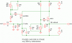
FOLDED CASCODE
Hallo,
I designed this I/V conversion based on PASSLABS circuits .
There is a thing that I do not find objectionable and I ask for help:
the fact is that the output drain dc point (at Q2)moves around into +/- 15 or so millivolts. Is it normal? Or is it a suspect of oscillation ?
All other points are dc stable.
Attachments
very good job...
Hi Klaus,
I am very interested to your tweak on the TDA1547, i've read all your posts about this project but i have to modify for my application in my CD10...
So i want to know the exact values in your schematic that you have used for the TDA1547... that's for you the values that give the best results...
I haven't at home an a 2sk389 but i want to test before with the only small fet that i have at the moment, the 2n4391...
after this i would like to do a diy-opamp (like Mr. Pass Pdf) for summing the differential channels of the two TDA and going out unbalanced...
Can you tell me the current values I1-I2-IL of your schematic? i think to make a test only making the current sources with the 2n4391... at the moment i haven't any irf610 o 9610...
I am also interested to the value of IL, and what have you used for the filter, RL and CL ( 55Khz?? ).
Have you used a +/- 30v supply?
thanks in advance for response and your schematic sharing...
Bye bye
Using the 2SK170's or 389's is an excellent idea, partly
because it improves the noise figure. To take full advantage
of such a thing, I think you want to use the same JFETS to
bias and to load the primary device, otherwise the Mosfet
noise will still intrude, not that it's much.
because it improves the noise figure. To take full advantage
of such a thing, I think you want to use the same JFETS to
bias and to load the primary device, otherwise the Mosfet
noise will still intrude, not that it's much.
Re: very good job...
Hi,
- the exact values in your schematic that you have used for the TDA1547...
Well, 4,75mA bias through 2SK389 stays. TDA1547 gives weak 0,075mA or so. It takes (like in the original data sheet) 13kOhm to get 1V peak. I used 10k, but it does not really matter. So at R_L with 13k 1mA is given at e.g. 13V bias voltage. 1mA + 4,75mA = 5,75mA at the upper CCS. 0,62V basis-emitter-voltage of the transistor at 5,75mA gives 108Ohms for the R.
I haven't at home an a 2sk389 but i want to test before with the only small fet that i have at the moment, the 2n4391...
--- be carefully. Compare the datasheets. For differnt JFETs the gate voltage is deviating very strongly. Some of them need almost exact 0V of gate voltage – you would have to change the schematic and lay the gate preloader between – and +.
I am also interested to the value of IL, and what have you used for the filter, RL and CL ( 55Khz?? ).
--- R_L is given by the DAC, it is the I/U work resistor. C_L must be adapted to this value to get ca. 55kHz. C = 1/(2pi*55kHz*R_L).
Have you used a +/- 30v supply?
--- I use +/- 27V, because I had lay a transformer like this around.
Regards
Klaus
thank you very much
... for the good exaustive explication ...
Probably i'll make exactly what you have do for the first stage, i've found a place where there is all the components that I haven't and fortunately a friend of mine orders many components all the weeks in this place, tomorrow i'll place an order for the 2sk389 and the others things...
For the differential stage for the moment i can use the original NE opamp... but I am thinking to do a dy-opamp like Mr Pass explicates on his document... it's sure that it will be a bit better than an op-amp...
the problem is that the IRF610 and the IRF9610 is out of production... and for the new components i can also ask for some samples free of charge...
Do you know somenthing to replace it with a good noise figure???
Thanks in advance
Bye
... for the good exaustive explication
...Probably i'll make exactly what you have do for the first stage, i've found a place where there is all the components that I haven't and fortunately a friend of mine orders many components all the weeks in this place, tomorrow i'll place an order for the 2sk389 and the others things...
For the differential stage for the moment i can use the original NE opamp... but I am thinking to do a dy-opamp like Mr Pass explicates on his document... it's sure that it will be a bit better than an op-amp...
the problem is that the IRF610 and the IRF9610 is out of production... and for the new components i can also ask for some samples free of charge...
Do you know somenthing to replace it with a good noise figure???
Thanks in advance
Bye
Hi DoctorWho70
You can find irf610 and irf9610 at http://www.rs-components.it/
A good choice can be ZVN3306A and ZVP3306A that are also less expensive.
For the balanced to unbalanced, you can use a very simple bosoz schematic, as I made in my pseudo D1 stage for my Teac VRDS8.
Ciao.
You can find irf610 and irf9610 at http://www.rs-components.it/
A good choice can be ZVN3306A and ZVP3306A that are also less expensive.
For the balanced to unbalanced, you can use a very simple bosoz schematic, as I made in my pseudo D1 stage for my Teac VRDS8.
Ciao.
I know the RS... but not for the good prices ...
So in the meantime i've probably found the 2sk386 to nedis.com, and i've got a malsane idea...
like mr Pass says, is using all 2sk389...
Implementing also CCS stages with a part of the 2sk389 with the simple source resistor... and finally to add the two differential channels and going out unbalanced, trying to replicate a schematic like yours but with this low noise fet...
Do you think that using this kind of current sources (wit a fet and a resistor) is worse than using a fet with a vbe reference or diodes or something similar?
Bye
...So in the meantime i've probably found the 2sk386 to nedis.com, and i've got a malsane idea...
like mr Pass says, is using all 2sk389...
Implementing also CCS stages with a part of the 2sk389 with the simple source resistor... and finally to add the two differential channels and going out unbalanced, trying to replicate a schematic like yours but with this low noise fet...
Do you think that using this kind of current sources (wit a fet and a resistor) is worse than using a fet with a vbe reference or diodes or something similar?
Bye
Re: Hi, Klaus !
Hi Arne,
no, I did not design&produce PCBs for this, I built up this circuit on a experiment board and did hard core wiring... A perfect layout, drawn on paper before, is mandatory, as well as tons of patience.
The TDA1547 was given in my commercial DAC, I just implemented this additional board.
Regards
Klaus
Cobra2 said:Have you made any PCB of the 1547 i/v converter?
Arne K
Hi Arne,
no, I did not design&produce PCBs for this, I built up this circuit on a experiment board and did hard core wiring... A perfect layout, drawn on paper before, is mandatory, as well as tons of patience.
The TDA1547 was given in my commercial DAC, I just implemented this additional board.
Regards
Klaus
Attachments
- Status
- This old topic is closed. If you want to reopen this topic, contact a moderator using the "Report Post" button.
- Home
- Amplifiers
- Pass Labs
- I/U stage D1 clone with 2sk389 finetuned...