I'm building a 6-channel integrated amp using a Hypex DLCP and 6x UcD400OEM modules. I posted a few questions in the Hypex DSP module(s) thread, but I've been feeling guilty about taking that thread off-topic by posting questions about interfacing to the UcD400OEM modules. So I thought I'd start a sort of build thread here, where I could ask some specific electronics questions.
I'm a novice at PCB designing, but since Hypex won't sell their OEM converter boards to non-OEMs, I've designed my own board. First samples are due in this week.
I've attempted to make use of the 'clipping', 'current limiting' and 'amplifier ready' signals, by including LEDs on my adapter board to show their status. But now I'd like to think about putting 3 status LEDs on my front panel, and I'm looking for help with the circuit design.
What I'd like is for:
1) A front panel LED to light if *any* of the individual UcDs is clipping
2) A front panel LED to light if *any* of the individual UcDs is current limiting
3) A front panel LED to light *only* if *all* the individual UcDs is ready.
So I'll start with the current limiting (CLIM) circuit. The documentation for the UcD400OEM says that the current limiting signal is internally pulled up (limited to 5.6V I think), and goes low (to -VB, i.e. -63V) when current limiting. So on my adapter board I connected an LED between the CLIM pin and ground, so that when the signal goes to -63V I get current through the LED. What I want now is to take all 6 CLIM signals to a front panel PCB with an LED that lights if any of these signals goes low. Would somebody be able to take a look at the schematic below and tell me if I'm on the right lines?
I would bring all the CLIM signals onto a 6-pin header JP1. LED1 to LED6 are the LEDs on my individual adapter boards. They are 10mA, 2V LEDs, so R1 to R6 are 6k1 - actually my board has two resistors in series for each of these resistors to give me flexibility over resistor values and power spec.
LED7 would be my front panel LED. D1 to D6 are diodes, because I think that if one pin goes low it would tend to pull all the others low as well, so the lights on each adapter would light. I'd rather that didn't happen, as I'd like to be able to look through the ventilation holes in the top of the enclosure to see which channel is current limiting. With those diodes I *think* I'd get only the LED on the corresponding adapter lighting up plus the one on the front panel.
Am I on the right lines? If so I think I can apply the same approach to the clipping signals (although they are the opposite way round: +63V normally, pulled to <=1V when clipping). The amplifier ready signals will take more effort I think, because I want a front panel LED that goes out if any of the amplifier ready lights goes out. Any suggestions for that one would be most welcome!
I'm a novice at PCB designing, but since Hypex won't sell their OEM converter boards to non-OEMs, I've designed my own board. First samples are due in this week.
An externally hosted image should be here but it was not working when we last tested it.
I've attempted to make use of the 'clipping', 'current limiting' and 'amplifier ready' signals, by including LEDs on my adapter board to show their status. But now I'd like to think about putting 3 status LEDs on my front panel, and I'm looking for help with the circuit design.
What I'd like is for:
1) A front panel LED to light if *any* of the individual UcDs is clipping
2) A front panel LED to light if *any* of the individual UcDs is current limiting
3) A front panel LED to light *only* if *all* the individual UcDs is ready.
So I'll start with the current limiting (CLIM) circuit. The documentation for the UcD400OEM says that the current limiting signal is internally pulled up (limited to 5.6V I think), and goes low (to -VB, i.e. -63V) when current limiting. So on my adapter board I connected an LED between the CLIM pin and ground, so that when the signal goes to -63V I get current through the LED. What I want now is to take all 6 CLIM signals to a front panel PCB with an LED that lights if any of these signals goes low. Would somebody be able to take a look at the schematic below and tell me if I'm on the right lines?
An externally hosted image should be here but it was not working when we last tested it.
I would bring all the CLIM signals onto a 6-pin header JP1. LED1 to LED6 are the LEDs on my individual adapter boards. They are 10mA, 2V LEDs, so R1 to R6 are 6k1 - actually my board has two resistors in series for each of these resistors to give me flexibility over resistor values and power spec.
LED7 would be my front panel LED. D1 to D6 are diodes, because I think that if one pin goes low it would tend to pull all the others low as well, so the lights on each adapter would light. I'd rather that didn't happen, as I'd like to be able to look through the ventilation holes in the top of the enclosure to see which channel is current limiting. With those diodes I *think* I'd get only the LED on the corresponding adapter lighting up plus the one on the front panel.
Am I on the right lines? If so I think I can apply the same approach to the clipping signals (although they are the opposite way round: +63V normally, pulled to <=1V when clipping). The amplifier ready signals will take more effort I think, because I want a front panel LED that goes out if any of the amplifier ready lights goes out. Any suggestions for that one would be most welcome!
Last edited:
My electronics knowledge is really limited, and I can't work out how to get a single 'Amplifiers Ready' LED that lights when every one of the individual 'Amp Ready' pins is at -VB, but which goes out if any of the pins goes high.
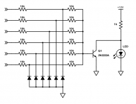
Hypex provide this diagram to describe the Amplifier Ready interface.
As far as I can tell, the transistor connects the Amp Ready pin to -VB via a 10k resistor when there's no error, but when there's an error it closes that path so that the Amp Ready pin is connected to +VB via a 1M resistor, but the voltage is limited to 5.6V by the zener diode.
So if 5 of my 6 amps are ok, but one has an error, then 5 are at -VB, via a combined resistance of 1/(5/10k) = 2k, and one is at +5.6V via a 1M resistor. So I think the 5 will win, i.e. one going high will not pull the others high - an LED controlled by tying these pins together would stay lit.
So I think some sort of logic is needed. My limited knowledge tells me that I could feed the front panel LED through 6 relays in series, each one switched by an individual one of the Amp Ready signals. So if one signal goes high the corresponding relay would open, so there'd be no circuit for the front panel LED. But 6 relays for one LED seems like overkill, and would be expensive. So there must be a better way.
I have a Raspberry Pi in the enclosure (acting as a Squeezebox server and player), and it possibly has 6 GPIO pins free, but I don't think I can monitor voltages of 63V.
So what about some sort of IC to handle the logic? Is there an easy way monitor the voltage of those 6 Amp Ready signals and only light my front panel LED when they're all at -VB?
Hypex provide this diagram to describe the Amplifier Ready interface.
An externally hosted image should be here but it was not working when we last tested it.
As far as I can tell, the transistor connects the Amp Ready pin to -VB via a 10k resistor when there's no error, but when there's an error it closes that path so that the Amp Ready pin is connected to +VB via a 1M resistor, but the voltage is limited to 5.6V by the zener diode.
So if 5 of my 6 amps are ok, but one has an error, then 5 are at -VB, via a combined resistance of 1/(5/10k) = 2k, and one is at +5.6V via a 1M resistor. So I think the 5 will win, i.e. one going high will not pull the others high - an LED controlled by tying these pins together would stay lit.
So I think some sort of logic is needed. My limited knowledge tells me that I could feed the front panel LED through 6 relays in series, each one switched by an individual one of the Amp Ready signals. So if one signal goes high the corresponding relay would open, so there'd be no circuit for the front panel LED. But 6 relays for one LED seems like overkill, and would be expensive. So there must be a better way.
I have a Raspberry Pi in the enclosure (acting as a Squeezebox server and player), and it possibly has 6 GPIO pins free, but I don't think I can monitor voltages of 63V.
So what about some sort of IC to handle the logic? Is there an easy way monitor the voltage of those 6 Amp Ready signals and only light my front panel LED when they're all at -VB?
Is there an easy way monitor the voltage of those 6 Amp Ready signals and only light my front panel LED when they're all at -VB?
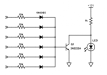
You need a six input NOR gate, something like this.
Attachments
Thank you, that's very helpful. I do appreciate your help, but my knowledge isn't good enough to take away a complete solution from that diagram.
Let me try to understand - are you suggesting I should use a 6-input NOR gate IC, and that diagram is simply an illustration of what the IC would do, or is that diagram something I could build from the discrete components shown, i.e. would I simply pass each 'amp ready' signal through a 10k resistor, then tie the outputs together as the base input to that transistor? Is 10k a value that you've selected to be suitable, given that each of my 'Amp Ready' signals will range from -63V ('ready') to +5.6V ('not ready')?
In the case of a single 'amp ready' signal going high to 5.6V, what would stop the other 5, at -63V, from pulling the tied output low?
Would I have to choose a transistor that can cope with -63V, or have those resistors brought the signals to acceptable levels?
My adapter board PCBs arrived today, earlier than expected. So I built one up with the components I've got so far - just waiting for the resistors to arrive now.
What have I learned? A few things:
1) I need to leave more room around the mounting holes! The resistors will fit, but they're too cramped for comfort. And there isn't room for the jumper that I was going to install between the 'DC Error' signal and the on-board pull-up resistor (top-left). In fact I worked out that there's no reason to ever disconnect that pull-up resistor, so I soldered a permanent link between those pads on the underside of the board. For the next version of the board I'll remove that jumper altogether - I can always leave the resistor out if necessary.
2) Soldering things that connect directly to the ground plane is more of a challenge than other components. I deliberately didn't use 'thermals' for the high current connections, but the ground plane and those fat traces certainly make for good heatsinks.
3) It doesn't matter how much I try to think through of all the details, there's always something I didn't think about. I wasn't really expecting to get it right first time - I'm sure there'll be other problems when I power it up. It's a good job that each iteration is relatively cheap.
I've made the adapter so that the amplifier modules will sit vertically, with their backs to the sides of the enclosure, where there'll be some hefty heatsinks.
I'm planning to use the Dissipante 3U enclosure from Modushop.biz.
Here's a mock-up of the current draft of the layout. The grid of crosses represents the optional baseplate for the Dissipante enclosure. The holes are at 10mm centres, so I've made all my boards with mounting holes to suit. The SMPS1200A400 has a mounting frame with holes that also suit the baseplate, but annoyingly the DLCP and SMPSDLCP have mounting holes that don't line up with the grid - I think I'll make separate mounting plates with holes that do align with the grid.
An externally hosted image should be here but it was not working when we last tested it.
What have I learned? A few things:
1) I need to leave more room around the mounting holes! The resistors will fit, but they're too cramped for comfort. And there isn't room for the jumper that I was going to install between the 'DC Error' signal and the on-board pull-up resistor (top-left). In fact I worked out that there's no reason to ever disconnect that pull-up resistor, so I soldered a permanent link between those pads on the underside of the board. For the next version of the board I'll remove that jumper altogether - I can always leave the resistor out if necessary.
2) Soldering things that connect directly to the ground plane is more of a challenge than other components. I deliberately didn't use 'thermals' for the high current connections, but the ground plane and those fat traces certainly make for good heatsinks.
3) It doesn't matter how much I try to think through of all the details, there's always something I didn't think about. I wasn't really expecting to get it right first time - I'm sure there'll be other problems when I power it up. It's a good job that each iteration is relatively cheap.
I've made the adapter so that the amplifier modules will sit vertically, with their backs to the sides of the enclosure, where there'll be some hefty heatsinks.
An externally hosted image should be here but it was not working when we last tested it.
I'm planning to use the Dissipante 3U enclosure from Modushop.biz.
Here's a mock-up of the current draft of the layout. The grid of crosses represents the optional baseplate for the Dissipante enclosure. The holes are at 10mm centres, so I've made all my boards with mounting holes to suit. The SMPS1200A400 has a mounting frame with holes that also suit the baseplate, but annoyingly the DLCP and SMPSDLCP have mounting holes that don't line up with the grid - I think I'll make separate mounting plates with holes that do align with the grid.
An externally hosted image should be here but it was not working when we last tested it.
Last edited:
In the case of a single 'amp ready' signal going high to 5.6V, what would stop
the other 5, at -63V, from pulling the tied output low?
Would I have to choose a transistor that can cope with -63V, or have those resistors
brought the signals to acceptable levels?
This is a NOR circuit. When any input(s) is (are) high, the transistor is on (collector is low).
Then the LED is off, because the 1k current is diverted from the LED by the transistor.
When all inputs are low, the transistor is off (collector is high), so the LED is supplied with
current through the 1k, and it lights up.
This circuit should work, except add a 1N4005 protection diode from the transistor base to ground
(cathode to base) to protect the BE junction from the negative input voltage. The 10k resistors
could be as large as 50k if you prefer.
Last edited:
Thank you, that's what I hoped you'd say!
But I still don't understand 'how' the 'NOR' part functions. I understand that the transistor diverts the current when its base is high, but what I don't understand is why the base will be high in a situation where 5 of the tied inputs are at -63V and only one of the inputs is at +5.6V.
How does -63V + -63V + -63V + -63V + -63V + 5.6V = 'high'?
Can't that single +5.6V find a path to the other -63V pins, with the net effect that the 6 tied inputs all end up 'low'?
I still don't understand 'how' the 'NOR' part functions.
Ok, this adds a clamp to ground for each input.
Attachments
I still don't understand 'how' the 'NOR' part functions.
In fact, just do it this way.
Attachments
Ah, now that one I can understand! Thank you, most appreciated.
In fact, I'm pretty sure that I've misinterpreted the way all three of these signals work (Amp Ready, Clipping and Current Limiting). I don't think they swing as low as -VB or as high as +VB - I think 'low' is at or near ground. So I think these pins aren't suitable to drive LEDs directly, but are intended only to switch an LED circuit, in a similar fashion to the circuit diagram you have kindly supplied. These LED circuits will need their own supply voltage, and I don't think +63V is the best place to start from, but that's the only voltage available on my adapter board. So I'm now planning to take these signals off-board to another board that will drive all of the LEDs, and I can use the auxiliary supply (+15.6V) on my SMPS to power the LEDs.
Your diagram has inspired me to do this properly with transistors. I have the option to have separate LEDs for each signal, so 6x Amp ready + 6x Clipping + 6x Current Limiting. Maybe I'll put those on the internal board, so I can take the lid off the enclosure and look at the status of each amplifier if I want to. But I'll also attempt to amalgamate these into 3 front panel LEDs:
- one showing when all 6 amplifiers are ready
- one showing if any of them is clipping
- and one showing if any of them is current limiting.
I'll use your diagram as a guide for how to do that.
After spending a while planning my off-board LED PCB, it was turning into a mammoth board with an extraordinary number of components just to light some LEDs. So I had another change of plan and moved the individual LEDs back onto the adapter board. I still plan to take each individual signal off to a separate board to make the 'amalgamated' front panel LEDs, but that should be a much simpler affair since it won't also have to include the 3x6 individual LEDs.
So I'll need to bring a separate LED driver supply onto the adapter boards, which I've labelled VDR in the attached diagram. I'll use a screw terminal block so that it's easy to daisy chain this supply to my 6 adapter boards.
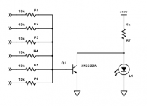
I'd appreciate a quick check on this schematic before I get too deeply into laying out the components on the PCB. R1, R3 and R5 are the current limiting resistors for the LEDs, with values TBD, R2, R4 and R6 are basically copied from Rayma's schematic - I guess they are current limiting for the transistors?? R7 is a pull-up resistor for the clipping signal - the other signals are internally pulled up. One thing I'd appreciate a check on is the relationship between R6 and R7 - which side of R6 should R7 connect? Looking at it now I think I may have it the wrong side.
So I'll need to bring a separate LED driver supply onto the adapter boards, which I've labelled VDR in the attached diagram. I'll use a screw terminal block so that it's easy to daisy chain this supply to my 6 adapter boards.
I'd appreciate a quick check on this schematic before I get too deeply into laying out the components on the PCB. R1, R3 and R5 are the current limiting resistors for the LEDs, with values TBD, R2, R4 and R6 are basically copied from Rayma's schematic - I guess they are current limiting for the transistors?? R7 is a pull-up resistor for the clipping signal - the other signals are internally pulled up. One thing I'd appreciate a check on is the relationship between R6 and R7 - which side of R6 should R7 connect? Looking at it now I think I may have it the wrong side.
An externally hosted image should be here but it was not working when we last tested it.
I'd appreciate a quick check on this schematic
This should need only one resistor connected to the 2N2222 base, around 10k.
Clarify again, is that input signal ground if "go", and high if "no go"?
R1, R3, R5 should be (Vcc-2V)/0.01A in ohms, and 2 x (Vcc-2V) x 0.01A in watts.
Last edited:
The pull up should need only one resistor connected to the 2N2222 base, around 10k.
So R7, but not R6? What's the purpose of R2 and R4? Are they not current limiting for the transistors, and if so, doesn't T3 also need R6 to do the same job?
So R7, but not R6? What's the purpose of R2 and R4? Are they not current limiting for
the transistors, and if so, doesn't T3 also need R6 to do the same job?
The series resistors R2, R4, R6 between the input and the base convert the input voltage signals to current,
which drives the BE junction, which causes the transistor to turn on and conduct enough current to saturate,
causing the collector voltage to fall to a low value, around 0.2VDC.
Last edited:
Clarify again, is that input signal ground if "go", and high if "no go"?
The clipping signal is normally high (due to the pull-up resistor) and goes low when the signal is clipping (which is when I want the LED to light).
The Current Limiting signal is internally pulled up (to 5.6V I think), and goes low when the amplifier is current limiting (which is when I want the LED to light).
The 'Ready' signal is normally low, but goes high (internally pulled up to 5.6V) when the amplifier has shut down due to an error (i.e. NOT ready). I want the LED to light when the amplifier is ready, i.e. when the signal is low.
The series resistors R2, R4, R6 between the input and the base convert the input voltage signals to current,
which drives the BE junction, which causes the transistor to turn on and conduct enough current to saturate,
causing the collector voltage to fall to a low value, around 0.2VDC.
Thank you - so shouldn't R6 be there to do the same job for T3? And I assumed R7 is needed as well because the clipping signal is an open collector which needs to be pulled up.
I want the LED to light when the amplifier is ready, i.e. when the signal is low.
So a "low" input always means the LED should be on. Then the circuit logic is correct.
Now we need to be sure of the logic levels so the circuit will properly function.
What is "low" and what is "high", in volts?
Thank you - so shouldn't R6 be there to do the same job for T3? And I assumed R7
is needed as well because the clipping signal is an open collector which needs to be pulled up.
Yes, all the transistors need the series resistor connected to the base.
Any open collector device needs a pull up resistor. Connect it before
the series base resistor (directly to the device), not after the resistor.
Last edited:
So a "low" input always means the LED should be on. Then the circuit logic is correct.
Now we need to be sure of the logic levels so the circuit will properly function.
What is "low" and what is "high", in volts?
Yes, that's right - in all three circuits, the LED needs to be on when the signal is low.
For the clipping signal, the open collector which I have to pull up, the notes say that the low state has a maximum of 1V. The pull up voltage must not exceed 65V (I'm planning to use 15.6V), and the maximum output current is 100mA.
For the current limiting signal, the low state apparently has a minimum value of -0.7V. It is internally pulled up to a value that I think is limited to 5.6V by a zener diode. I'll post the schematic in a moment.
For the Amplifier Ready signal, the low state apparently has a minimum value of -0.6V. It is internally pulled up to 5.6V (similar schematic to the current limiting signal).
Yes, all the transistors need the series resistor connected to the base.
Any open collector device needs a pull up resistor. Connect it before
the series base resistor (directly to the device), not after the resistor.
Thank you - that makes sense. So I had it wrong in my earlier schematic, as I suspected.
- Status
- This old topic is closed. If you want to reopen this topic, contact a moderator using the "Report Post" button.
- Home
- Amplifiers
- Class D
- Hypex DLCP/UcD400 build