i'm trying to create an ad844 dac based on http://www.diyaudio.com/forums/digital-source/227677-using-ad844-i-v.html
rough block diagram as seen on the pic. currently only tried it on a breadboard but every iteration i've made so far has a lot of noise.
there's a high pitched hum when i2s is fed to the dac chips- otherwise the whole thing is silent when cs8412 is taken out.
then there's high pitched noise that modulates with high frequency signal- when 12khz, 14khz (and above) tones are played, 8khz (ish, i'm not so sure) noise is overlaid with the signal. this is also heard in the music, obviously.
then there's static noise with the right channel signal of the dac. this is a radio static-like noise that gets excited with the music. and no matter what i swap it is always with the right signal so the noise is in the signal domain- a design error, not a construction error.
as you can see in the diagram, i've tried to bias the - input of ad844 with the negative polarity of tda1387 in a differential mode, instead of zero dc offset then input to the ground as it is done in the original ad844 thread. i only get about 10mv offset at the pin 5 output of ad844. but with horrible sound as described above....
what have i done wrong? i've breadboarded george's ad844 implementations before and they all came out wonderful.
everything is properly decoupled on the board and the ad844 i/v resistors are paralleled with 1nf caps.
free picture upload
rough block diagram as seen on the pic. currently only tried it on a breadboard but every iteration i've made so far has a lot of noise.
there's a high pitched hum when i2s is fed to the dac chips- otherwise the whole thing is silent when cs8412 is taken out.
then there's high pitched noise that modulates with high frequency signal- when 12khz, 14khz (and above) tones are played, 8khz (ish, i'm not so sure) noise is overlaid with the signal. this is also heard in the music, obviously.
then there's static noise with the right channel signal of the dac. this is a radio static-like noise that gets excited with the music. and no matter what i swap it is always with the right signal so the noise is in the signal domain- a design error, not a construction error.
as you can see in the diagram, i've tried to bias the - input of ad844 with the negative polarity of tda1387 in a differential mode, instead of zero dc offset then input to the ground as it is done in the original ad844 thread. i only get about 10mv offset at the pin 5 output of ad844. but with horrible sound as described above....
what have i done wrong? i've breadboarded george's ad844 implementations before and they all came out wonderful.
everything is properly decoupled on the board and the ad844 i/v resistors are paralleled with 1nf caps.
An externally hosted image should be here but it was not working when we last tested it.
free picture upload
Last edited:
An externally hosted image should be here but it was not working when we last tested it.
sorry, abraxaito, i don't know how to draw schematics, and the implementation is crude as it is. it's basically differential tda1387 with ad844 i/v stage as described above.
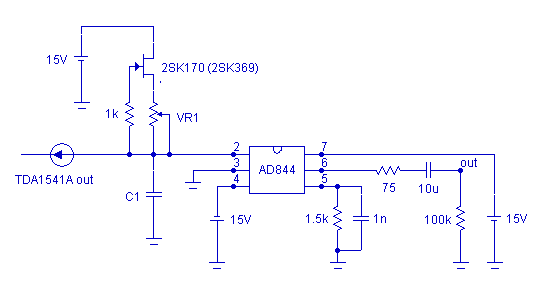
no different from this except pin 3 gets fed negative phase signal instead of going to ground, and no dc offset circuit.
no different from this except pin 3 gets fed negative phase signal instead of going to ground, and no dc offset circuit.
If you connect pin3 of the AD844 to one of the outputs of the TDA1387, you'll have a problem if there's no resistor to convert the I to V. Also probably the JFET current source is providing too much current - just a guess. A circuit for the TDA1541A isn't going to be directly compatible with TDA1387.
Does it get better or worse when you short pin 3 to ground, making it single-ended?
The DAC chip has a large output voltage compliance (0 to 3.5 V), so maybe you can indeed use a resistor rather than a virtual ground on one of the outputs. Still, the application schematic shows a virtual ground, so that probably works better.
If the noises you hear are soft background tones/noises, they could be due to some crosstalk on your breadboard. Have you tried minimizing loop areas, using a ground plane and keeping analogue and digital loops separated where possible?
Assuming you're still running your AD844 on +15/-15V supplies then if pin3 is set to 0V the DAC's output will be unipolar, always more -ve than 0V. So to get a bipolar output you'll need to add in a current source to the negative rail (to pin2) or alternatively raise the voltage at pin3 above 0V.
If for example you were going for a standard CD level output (2VRMS) then your feedback resistor (pin6 to pin2) should be 5.6k and you'll want a 2.8V reference at pin3. You could achieve this with a TL431 and appropriate resistors - 3k ref to a and 330R k to ref.
If for example you were going for a standard CD level output (2VRMS) then your feedback resistor (pin6 to pin2) should be 5.6k and you'll want a 2.8V reference at pin3. You could achieve this with a TL431 and appropriate resistors - 3k ref to a and 330R k to ref.
Thank you abralaxito. Now im playing with just passive iv 1387 and cant believe how good it sounds.
What is the lowest iv value the chip can take? Currently have 2.7k ohm to ad797 unity gain buffer but im wondering if something like 50ohm > opamp gain will improve the dynamics.
What is the lowest iv value the chip can take? Currently have 2.7k ohm to ad797 unity gain buffer but im wondering if something like 50ohm > opamp gain will improve the dynamics.
Also, going back to ad844, if i want a current source at pin2, which circuit should i try? And can either solutions u listed work wihout the feedback resistor to make it the way george uses it in his ad844 i/v thread?
1387 has a vref pin.... does it have any secret uses here? Hehe
1387 has a vref pin.... does it have any secret uses here? Hehe
You can go as low as you like for the I/V resistor but in my experience going lower doesn't improve the dynamics. The reason for this I reckon is that dynamics are limited by the on-chip current sources (between outputs and VDD) - these 'leak' noise from the supply.
To get better dynamics I had to go to active I/V - but not with opamps as they're not classA. You can use simply a common-base transistor but its input impedance won't be extremely low without at least 10mA of current. Or you can use feedback to lower the input impedance - there's a discrete classA CFB I/V schematic shown on my blog, I've had great results with that. The active I/V effectively puts a very low value of I/V resistor on the DAC but without the need for large voltage gain afterwards.
For current sources I use the 2 transistor configuration which is very common. Pin7 is Vref - it benefits from a lot of capacitance for good bass - use at least 1,000uF.
- Status
- This old topic is closed. If you want to reopen this topic, contact a moderator using the "Report Post" button.
- Home
- Source & Line
- Digital Line Level
- help me with my dac design?