Hi all,
My Classe 25 (probably a VERY early one given that the PCB designators match the DR-25) has developed a problem on one channel. Resistor R17 (R19 on my amp) on the PCB found in this package has burned:
http://bwgroupsupport.com/downloads/techmanuals/classe/DR-25-Model 25-TM.pdf
Because this is a voltage dropper for the front end of the output stage, I'm hoping that the fault lies before the output transistors as they look like they would be a real chore to get out for individual testing! The other channel works fine. I have limited experience with discrete solid state power amps, so any suggestions on where I should start looking would be most welcome.
Thanks!
Bumping this thread as I want to get back to fixing this amp! I would appreciate it if someone could point me in a direction to start looking at what may be causing this issue! In-circuit checking of all diodes and transistors looks good.
Thank you for your help!
Thank you for your help!
Attachments
I'd suspect C15. 100 V electrolytic, >80 V rails, seems a bit tight if you ask me (depending on what they used). Do you find any measurable shorts after the dead resistor? Anyway, high-voltage breakdown faults can be hard to find.
BTW, I think Q6 and Q7 on the schematic are reversed.
BTW, I think Q6 and Q7 on the schematic are reversed.
That resistor mainly isolates the power devices from the rest of the amp circuitry. If it smoked, something to the left of the resistor is faulty. Resistance testing should turn up something rather quickly, with one probe on C15 (+) and the other at various positions in the amplifier.
If simple resistance checking doesn't turn up anything, I would continue by checking any SMD capacitors, as they are known to fail brilliantly in some of the Classe designs.
If simple resistance checking doesn't turn up anything, I would continue by checking any SMD capacitors, as they are known to fail brilliantly in some of the Classe designs.
I'd suspect C15. 100 V electrolytic, >80 V rails, seems a bit tight if you ask me (depending on what they used). Do you find any measurable shorts after the dead resistor? Anyway, high-voltage breakdown faults can be hard to find.
BTW, I think Q6 and Q7 on the schematic are reversed.
Hi,
C15 is fine and so are all other capacitors on that channel. Interesting to hear your comment about Q6 and Q7...I doubled checked and absolutely they are connected as per the schematic. My early Model 25 has a number of differences from the published schematic and it looks like the earlier version of the PCB was designed to use TO-92 devices in both the Q6 and Q7 positions. The MJE350 and MJE340 devices have twisted legs to fit in the TO-92 footprint and have small heat sinks attached to them. On the later version of this amp the PCB was revised and these devices are mounted directly to the main heat sink. I wonder if they messed up originally and have MJE350 in the wrong position? So far I see no shorts to suggest why that resistor is burning...any other suggestions on where I might look? Is there any harm in lifting the VCC sides of the 33R2 resistors from both rails and powering up through a current limited bench supply without the drive and output transistors being powered?
Hmm. Any signs of shorting? As I said, high-voltage breakdown faults can be tricky to find.C15 is fine and so are all other capacitors on that channel.
So the one that connects to R11 is Q6 and it is an MJE350, and Q7 is the MPSA56?Interesting to hear your comment about Q6 and Q7...I doubled checked and absolutely they are connected as per the schematic.
That makes no *******' sense though. Q6/7 basically form a cascode current source to go with the cascode VAS involving Q9/10. The fun part of a cascode is that the lower device (like Q10) can be a high-beta, low-capacitance job rated at a relatively modest breakdown voltage, while the characteristics of the upper one (like Q9) are a fair bit less critical, so you can use a more robust part there. They're even using a bootstrapped bias connection on Q9 to further reduce its influence. For a pnp, the "lower" device has to become the "upper" one, of course.
The rated breakdown voltage of an MPSA56 is 80 V (vs. the 300 V of an MJE350). Your amp has nominal +/-84.2 V supplies, it might see 140-160 V peak-peak at full power (not to mention some thermal abuse). That it has survived for as long as it did is a small miracle in itself. Even if it does not measure dead short C-E as-is, it's going to be degraded and should be replaced while correcting the transistor mixup goof.
Q7 biasing via R10 also looks extremely dodgy to me, it's relying on transistor beta to set emitter voltage, and that's definitely not how it should be done (beta tends to be quite variable). All assuming the schematic is correct. I'd rather see an LED with ~100 µF in parallel (giving anything from 1.8-1.9 V for red to ~3 V below VCC+ for blue/white), biased from ground via ~47k or VCC- via 2x 47k in series or 1x 100k (observe voltage rating!), going to Q7 base via ~220 ohms.
Seems so. Guess the schematics guy goofed and the layout/parts person took their word for it. Now how stupid is that.I wonder if they messed up originally and have MJE350 in the wrong position?
Any fully DC-coupled amp like this is not going to work without its frontend. The output would go to one rail and you may end up blowing up poor little C9 and possibly damaging some of the input transistors as well. I'd just poke around with the resistance test as suggested.Is there any harm in lifting the VCC sides of the 33R2 resistors from both rails and powering up through a current limited bench supply without the drive and output transistors being powered?
Last edited:
Well, you have already done resistance testing. R17 smoked because there was a low resistance to ground. Does R18 show signs of overheating? Zobel network show signs of overheating? Does R17 smoke instantly after it is replaced?
In this case I would replace R17 and R18 with 100 ohm resistors and see which parts are running warm. No load connected, of course.
What is the meaning of the 4 x 100K resistors? This arrangement is not seen in other designs. Why are the c.s. diodes D1 and D2 connected to V- instead of ground?
If you don't get any clues, you will have to bring up V+ and V- slowly starting at about 30 volts. On this type of untested and unique design, you can't assume everything will power up the way you think it does. Various transistors can saturate while the supply is still increasing - all based on variations in part tolerance. My theory is still small value capacitors short circuit. +/- 85 volts is pushing it a little don't you think?
Another way to approach this problem is with a differential probe connected accross various parts - watch the response during power-up. Sometimes you have to let something fail to direct your attention to the problem.
RA
What is the meaning of the 4 x 100K resistors?
Set the required ccs current by inserting as many resistors in the board as needed?
Yes, I have checked every capacitor in circuit, each resistor value, and each transistor for shorts. I have NOT pulled all the of the parts to check them at this point, but that might be my next step. I have also checked continuity on every circuit trace to look for broken pads or traces or bad solder joints. Output Zobel is also fine. Frustratingly everything checks out ok. I think at this point I will bring up the working channel on a variac until the rails reach +/-40VDC or so (half full rail voltage) and make detailed voltage measurements at all transistor junctions. I will then do the same with the bad channel, unless I see a huge current draw on the positive rail, or R17 starts smoking. I should note that R18 shows no signs of heat damage, but R16 and the paralleled combo of R20/R9/R7 show some discoloration. They measure fine and the working channel shows the same amount of discoloration on those parts. Once I get this amp fully working again I will look at replacing those parts with higher wattage versions and stand them slightly off the PCB.
Thanks everyone for your suggestions so far!
Thanks everyone for your suggestions so far!
Well, you have already done resistance testing. R17 smoked because there was a low resistance to ground. Does R18 show signs of overheating? Zobel network show signs of overheating? Does R17 smoke instantly after it is replaced?
In this case I would replace R17 and R18 with 100 ohm resistors and see which parts are running warm. No load connected, of course.
What is the meaning of the 4 x 100K resistors? This arrangement is not seen in other designs. Why are the c.s. diodes D1 and D2 connected to V- instead of ground?
If you don't get any clues, you will have to bring up V+ and V- slowly starting at about 30 volts. On this type of untested and unique design, you can't assume everything will power up the way you think it does. Various transistors can saturate while the supply is still increasing - all based on variations in part tolerance. My theory is still small value capacitors short circuit. +/- 85 volts is pushing it a little don't you think?
Another way to approach this problem is with a differential probe connected accross various parts - watch the response during power-up. Sometimes you have to let something fail to direct your attention to the problem.
RA
Well of course that is the function of 4 paralleled 100K resistors - which are tied to V- in a very un-traditional way. It just is not apparent what is gained, over tying the resistors (of proper value) to ground at the point. The diodes are still providing 1.2v of bias to the ccs.Set the required ccs current by inserting as many resistors in the board as needed?
2 x 85v = 170v between the rails
4 100K in parallel = 25K total
current through diodes is (170v - 1.2v)/25K = 7mA + base currents from 3 transistors. But then with Classe, you always get innovation first, over reliability. Marketing.
RA
I really do not believe in this method of troubleshooting. I think you can rely on your reason to come up with better ways to approach this problem. Besides, indications are that there may not be a failed part. Just look at this design! So...what happens when you put a new 33 ohm resistor in? Have you tried 2 100 ohm resistors in their place? (or greater if you are uneasy about it).I have NOT pulled all the of the parts to check them at this point, but that might be my next step.
a good plan. I think you will come up with some good information.I have also checked continuity on every circuit trace to look for broken pads or traces or bad solder joints. Output Zobel is also fine. Frustratingly everything checks out ok. I think at this point I will bring up the working channel on a variac until the rails reach +/-40VDC or so (half full rail voltage) and make detailed voltage measurements at all transistor junctions. I will then do the same with the bad channel
RA
Additionally, why do you suppose the input stage does not have a current mirror load, like almost every modern design? Notice all the small value bypass caps, most of which consist of 2 in series. Do you really need to bypass resistors that are there to swamp beta variations?
If you have a capacitance meter, see if you get a close value for all those bypass caps, which I believe are all SMD parts.
RA
If you have a capacitance meter, see if you get a close value for all those bypass caps, which I believe are all SMD parts.
RA
Well, I hate to admit this, but I think I have found a (the?) problem. Originally I had disconnected the bad channel side from the power supply and checked voltages. They were all close to being correct, as I remember it. As I am now going through each section of the amplifier, I disconnected the power connections from the working channel, just so I could check the entire power supply on its own...and there I found a problem. The main filter capacitor for the positive supply of the BAD channel with the burned resistor is open! I removed it from the amplifier and checked it on its own and it is definitely bad...failed open circuit. Now...this suggests that the channel with the smoked resistor on the positive rail was getting rectified but unfiltered DC. Now, my concern is trying to understand if the bad cap caused damage to the amp channel with the smoked resistor, or if something on the bad channel caused the cap to be damaged? I have a suitable cap to wire in as a temporary replacement and I will confirm that the power supply is working correct before connecting up the channels and checking everything at a low line voltage first (Classe says to start at 10VAC in the service manual). I'd like to know if there is anywhere else I should look closely for damage before applying power?
Thanks!
Thanks!
OK, time to update my saga with this amplifier and disseminate some much needed information in case anyone searches for servicing help on these amplifiers. First off, the "bad" channel is working perfectly now. I have run it for many hours at low bias (14 ma across 0.27 ohms) on my bench, raised the bias to the suggested 22ma and all is still fine after an hour. The culprits turned out to be BOTH main filter capacitors on that channel. One was completely open and the other shows signs of serious leakage as it will not hold charge. At the moment I had to wire in some snap-in type caps to make sure the amp channel itself is working, which thankfully it is.
Now, on to the many mysteries:
Although my amp is marked Model 25, it looks to actually be a DR25 internally. There are significant differences between the two in terms of PCBs, designators, etc., which was making it nearly impossible to understand at first from the service manual. The service manual that is available from B&W Group is only for the later Model 25. The way to tell is that the MJE340 and MJE350 are mounted directly to the main heatsink. More on this in a moment.
Once I discovered the PCB differences, I found that the front end of all of Classe amps of this vintage, and the earlier DR9 and DR8 are nearly identical. Looking at the schematic for the DR15 shows that the designators line up exactly with my amp...apparently a DR25. Basically, to design the DR25, it looks like Dave Reich took the design of the DR9, upped the supply voltages, changed parts as required surrounding the input LTP, VAS, and driver stages for those higher supply voltages, gave us more power (250 wpc instead of a very conservative 100 wpc for the DR9) and lost the ability to drive 2 ohms loads comfortably. The earlier DR8 and DR9 used cascoded MPSA06s for the VAS and cascoded MPSA56s for the VAS current source. From what I can determine through lots of Google searching, is that this was a point of failure for those amplifiers. I expect that is why Q6 and Q9 were changed from MPSA56/MPSA06 to MJE350/MJE340 and heat sinks attached. However, I gather that there was also a problem with the early DR25s like mine as Q6 and Q9, despite their small heat sinks, run VERY hot. I measured 92 degrees Celsius on both of these devices after a couple hours of idling, even with the top removed! This is uncomfortably hot for these devices, hence the reason that the updated Model 25 PCB moved their locations so that they could me mounted directly to the main heat sink.
Oh, I forgot to mention the main filter capacitors...it's a wonder that they lasted so many years given that they are rated for 80V and the amplifier rails measure 82V with a 120VAC input! I am going to replace them with slightly smaller value 24,000uF/100V cans, as soon as they are back in stock at Digikey. While I have already gone to the trouble of disassembling half of this monster, and have to replace parts anyway, I'm am naturally going to replace all four of the main filter caps, all the electrolytics on the soft start, input, DC protection, and main amp boards, possibly look at hot-rodding the RCA inputs to bypass the Balanced and Bridging switching, and maybe the input buffers. The final step will be to find a more suitable heat sinking arrangement for Q6 and Q9 so that the amp does not decide to self-destruct someday. Any advice/recommendations for other possible improvements would be most welcome!
Last edited:
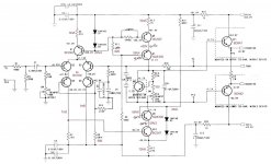
I have attached a marked-up front end schematic that is correct for the DR-25 and very early Model 25s like my unit. It is nearly identical in topology to the DR-15, so much so that I have actually used the DR-15 schematic as a mark-up reference. All voltages were measured with a stable 120VAC line and bias set to minimum. You will note that there are significant differences to the schematic that I posted earlier which was taken from the Classe published service manual. Unfortunately, since the takeover of Classe by the B&W Group, there is little knowledge remaining about these early Classe models, which I why I have continued to update this thread. I am interested in correcting (reversing) the position of Q6 and Q7 (MJE 350 and MPSA56) to improve reliability as I am already going to have to spend money to replace all of the electrolytic capacitors. As suggested in another thread, I gather that to reverse the Q6 and Q7 devices I should change R9 to 820 ohms and short R10? Also, would it be beneficial to replace C4 on both channels with something "audio grade" such as Elna Silmic II or Nichicon Muse?
Thanks!
Thanks!
Attachments
Last edited:
In other interesting news, I contacted Classe service (actually B&W Group service) to question the incorrectly specified original filter capacitors and to see if they had suitable replacements. Their response was to suggest that these were not the original capacitors (!) and that someone must have serviced the amp with the wrong parts. This is despite that fact that the original caps are marked as custom Classe parts of the correct vintage and I have a production document from Classe showing that the DR-25 rail voltage is +/- 81.5V and that 30,000uF/80V capacitors should be installed. Classe does have correct 30,000uF/90V replacements available for $150 USD...EACH! I'm going to replace these with new UCC 27,000uF/100V high ripple current parts for less than $30 USD each.
Your DR25 also shows 62volts not 81v ?
That is like the model 15.This is what i proposed as changes.
Tryed to use, as much as possible, the resistor values allready used.
Mona
No, my DR-25 has rail voltages of +/-82V. Otherwise it is very similar to the DR-15 front end, only a few resistor values are different. You can see everything in my attached schematic which corresponds precisely to my unit.
Thanks!
And that is why everyone moved on from this thread. The first step is ALWAYS to check the power supply. You were way past that point right from the beginning.OK, time to update my saga with this amplifier and disseminate some much needed information in case anyone searches for servicing help on these amplifiers. First off, the "bad" channel is working perfectly now. I have run it for many hours at low bias (14 ma across 0.27 ohms) on my bench, raised the bias to the suggested 22ma and all is still fine after an hour. The culprits turned out to be BOTH main filter capacitors on that channel. One was completely open and the other shows signs of serious leakage as it will not hold charge. At the moment I had to wire in some snap-in type caps to make sure the amp channel itself is working, which thankfully it is.
Doesn't surprise me a bit. As I said, what you get with Classe is styling and innovation at the expense of, well, reliable and tested designs.Although my amp is marked Model 25, it looks to actually be a DR25 internally. There are significant differences between the two in terms of PCBs, designators, etc., which was making it nearly impossible to understand at first from the service manual. The service manual that is available from B&W Group is only for the later Model 25. The way to tell is that the MJE340 and MJE350 are mounted directly to the main heatsink. More on this in a moment.
Most designs REQUIRE that the cover be on the unit to achieve the designed air flow past the heat sinks. This design may still be lacking, but just understand that running it with the cabinet off will almost always mean higher heat.This is uncomfortably hot for these devices, hence the reason that the updated Model 25 PCB moved their locations so that they could me mounted directly to the main heat sink.
Well that's certainly a tall order unless you have nothing better to do. Replace your incorrectly specified main filters and re-assess. There is really no need to start replacing everything in sight. I wouldn't stress over the Q6/Q9 problem. Why start re-designing the unit? Put in a cooling fan and maybe a vent and you are done. Popping in different transistors won't make it produce less heat. You simply need to remove the heat more efficiently.I'm am naturally going to replace all four of the main filter caps, all the electrolytics on the soft start, input, DC protection, and main amp boards, possibly look at hot-rodding the RCA inputs to bypass the Balanced and Bridging switching, and maybe the input buffers. The final step will be to find a more suitable heat sinking arrangement for Q6 and Q9 so that the amp does not decide to self-destruct someday. Any advice/recommendations for other possible improvements would be most welcome!
RA
- Status
- This old topic is closed. If you want to reopen this topic, contact a moderator using the "Report Post" button.
- Home
- Amplifiers
- Solid State
- Classe DR-25/25 repair