Hi guys,
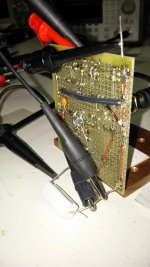
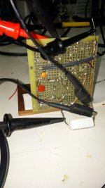
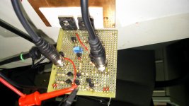
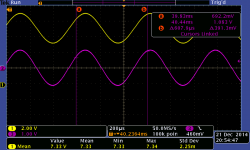
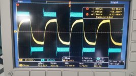
I am an electronics engineer that usually deals with non audio class d amplifiers. I just recently got interested in linear audio amplifiers and was intrigued by the how low cost a basic linear amp can be to thrown together. So after a bunch of reading through the forum and the art of electronics, I put together this amp which I spiced in LTspice and all seems well. It has pretty much all the basic parts that seem to be pretty common so I think you guys will be able to help. Initial start-up, It has high frequency oscillations so I increase the miller compensation cap. Surprisingly it needs to be much higher than ltspice says to become stable. The second problem and currently the biggest problem is that there is a 7.3V positive dc offset on the output. I tried messing with most stuff like the current sources by probing resistors in parallel. I tried finger probing around to find a location that finger resistance and capacitance would tweak the circuit response. Everything resulted in an identical output except altering the 3k feedback resistor. When I decrease the feedback resistor the AC gain decreases as expected but the DC offset also decreases, it seems by the same proportional amount. The AC gain is also completely wrong. It is supposed to be around 30 and it looks like the gain is around 2. I built this on a whim so it is powered by +-12v 6A laptop style supplies. I also intended on using 2n5551 NPN transistors but couldn't find them for the build so they are all 2n3904s which appears ok with low rails. I also have 2sd2390 and 2SB1560 on the final output stage. These are all what I had available to build with without ordering anything. I have no intentions on getting prefect hifi on this build I just want to get it working to play with. I probed the the -diff input transistor and it looks like a perfected 0VDC sinewave so interestingly it looks like the feedback thinks its working. DC on the output side of the 3k and no DC on the BJT side. Looking at the scope screenshot the yellow trace is the output and the magenta trace is the input. Also attached is the simulation I designed from and pics of the build. I think some of you guys will be able to quickly pick out my problem. I am looking forward to any thoughts. Thanks.
I am an electronics engineer that usually deals with non audio class d amplifiers. I just recently got interested in linear audio amplifiers and was intrigued by the how low cost a basic linear amp can be to thrown together. So after a bunch of reading through the forum and the art of electronics, I put together this amp which I spiced in LTspice and all seems well. It has pretty much all the basic parts that seem to be pretty common so I think you guys will be able to help. Initial start-up, It has high frequency oscillations so I increase the miller compensation cap. Surprisingly it needs to be much higher than ltspice says to become stable. The second problem and currently the biggest problem is that there is a 7.3V positive dc offset on the output. I tried messing with most stuff like the current sources by probing resistors in parallel. I tried finger probing around to find a location that finger resistance and capacitance would tweak the circuit response. Everything resulted in an identical output except altering the 3k feedback resistor. When I decrease the feedback resistor the AC gain decreases as expected but the DC offset also decreases, it seems by the same proportional amount. The AC gain is also completely wrong. It is supposed to be around 30 and it looks like the gain is around 2. I built this on a whim so it is powered by +-12v 6A laptop style supplies. I also intended on using 2n5551 NPN transistors but couldn't find them for the build so they are all 2n3904s which appears ok with low rails. I also have 2sd2390 and 2SB1560 on the final output stage. These are all what I had available to build with without ordering anything. I have no intentions on getting prefect hifi on this build I just want to get it working to play with. I probed the the -diff input transistor and it looks like a perfected 0VDC sinewave so interestingly it looks like the feedback thinks its working. DC on the output side of the 3k and no DC on the BJT side. Looking at the scope screenshot the yellow trace is the output and the magenta trace is the input. Also attached is the simulation I designed from and pics of the build. I think some of you guys will be able to quickly pick out my problem. I am looking forward to any thoughts. Thanks.
Attachments
Try adding a capacitor between your 90ohm ? feedback resistor and ground. Having it grounded directly will cause large offsets unless the ltp transistors are perfectly matched. Also the resistor on the input side from base to ground should be the same value, can,t see it from the pic since it,s standing up. I would go with 10k's for this one and the feedback one going to output, 3k is a little low since this will define input impedance, and 560 for the smaller feedback resistor with 100uF capacitor to ground.
Last edited:
Jerluwoo,
Thanks for the tip. I do recall seeing that cap on other ac coupled amps. I gave it a try with mixed results. I put in a 470uf in series with the 100r to ground and it did seem to correct the dc as the cap charged. So at power on it had the 7v dc offset and then charged down toward 0v. The problem is once the sine wave crossed 0v it clipped the bottom of the wave. So that kinda bandaids the problem. But there seems to be a bigger issue.
Other updates and tests-
Added 500r trimpot to the emitters of the ltp with the wiper going to the ccs to the neg rail. I was able to get +-2v of dc offset adjustment but not enough.
I added a 4700uf cap to the output and so I could connect up a speaker. It seemed to drive them great. I was able to get ~25w into the 1.7ohm paralleled speakers before clipping. Though I think when everything is working right I think I should be able to get closer to 40w.
Switching to my phone as a signal source, it drove fine other than the fact that the phone can't drive more than like 200mv pk so it didn't get very loud with the phone all the way up. So that brought me back to the gain problem. It still only has a ac gain of 2 when it should be 30. I increased the negative feedback resistor to 10k from 3k so theoretical gain of 100. It resulted with the dc offset being completely in the positive rail and I had to put a negative offset on the function generator to get the wave into driving range. It did not increase the ac gain much at all.
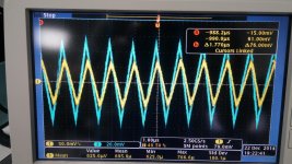
I was very impressed with the speed of the amp . I tested square and triangle waves up to 1mhz and they looked Damn good with only some slew distortion and some hf hash in which might be coming from the test equipment because the hash was on the input signal from the agilent function generator. The input waves are blue and the outputs are yellow. The out is ac coupled on the scope. This was a low voltage test so the slews will probably get worse at high voltage. Way faster than audio needs but I might drive some piezo transducers with it at work.
Counter culture,
I will get that first post cleaned up. I spewed all my thoughts through my phone. Which is more difficult to format. Sorry for these first post lengths also I'm just trying to get enough info on here to get the correct help.
Im hoping that I get get some more advice and help. I'm eager to get a second one working to have stereo. Thanks in advance.
Thanks for the tip. I do recall seeing that cap on other ac coupled amps. I gave it a try with mixed results. I put in a 470uf in series with the 100r to ground and it did seem to correct the dc as the cap charged. So at power on it had the 7v dc offset and then charged down toward 0v. The problem is once the sine wave crossed 0v it clipped the bottom of the wave. So that kinda bandaids the problem. But there seems to be a bigger issue.
Other updates and tests-
Added 500r trimpot to the emitters of the ltp with the wiper going to the ccs to the neg rail. I was able to get +-2v of dc offset adjustment but not enough.
I added a 4700uf cap to the output and so I could connect up a speaker. It seemed to drive them great. I was able to get ~25w into the 1.7ohm paralleled speakers before clipping. Though I think when everything is working right I think I should be able to get closer to 40w.
Switching to my phone as a signal source, it drove fine other than the fact that the phone can't drive more than like 200mv pk so it didn't get very loud with the phone all the way up. So that brought me back to the gain problem. It still only has a ac gain of 2 when it should be 30. I increased the negative feedback resistor to 10k from 3k so theoretical gain of 100. It resulted with the dc offset being completely in the positive rail and I had to put a negative offset on the function generator to get the wave into driving range. It did not increase the ac gain much at all.
I was very impressed with the speed of the amp . I tested square and triangle waves up to 1mhz and they looked Damn good with only some slew distortion and some hf hash in which might be coming from the test equipment because the hash was on the input signal from the agilent function generator. The input waves are blue and the outputs are yellow. The out is ac coupled on the scope. This was a low voltage test so the slews will probably get worse at high voltage. Way faster than audio needs but I might drive some piezo transducers with it at work.
Counter culture,
I will get that first post cleaned up. I spewed all my thoughts through my phone. Which is more difficult to format. Sorry for these first post lengths also I'm just trying to get enough info on here to get the correct help.
Im hoping that I get get some more advice and help. I'm eager to get a second one working to have stereo. Thanks in advance.
Attachments
My tuppence worth -
1 - that D45H11 (?) PNP transistor is no compliment of the 2N3055 that I know of - try MJ2955.
2 - You have no emitter degeneration resistors nor base resistors in output stage. Suggest you start off with 0.47 ohms in series with each output transistor emitter and circa 100 ohms in series with their bases. You can then reduce to 0.22R min recommended emitter resistors and a token base resistor that helps with thermal stability...
attached is modified schematic.... some component values are up for tweaking!
Don't forget with DC coupled input this will pass any input DC offset on to the output!
Attachments
Last edited:
Blu_Glo,
1 - These were the only 10A transistors in my ltspice library. I am not really using them in the real circuit. I am using sanken audio darlingtons 2SD2390 and 2SB1560 of which I don't have spice models to.
2 - I'm under the impression that the 100ohm base resistors are only necessary if there is a emitter follower frequency stability issue or to linearize vbe differences when paralleling output devices. I also assumed since that I was using a single output stage that the emitter resistor wasn't necessary because current sharing wasn't needed like in a parallel output setup. I do think I should put them in to stabilize the bias current.
There are some questions about some of your tweaks that I don't understand.
1. Can you explain C6 and R20? I have never seen them used that way. C6 breaks the necessary connection point for R9 which breaks the VBE multiplier. There is 6V of bias in your version causing 2A of bias current in the output stage.
2. What was wrong with the 4.7k resistors in the current sources? You have changed them to 10k but I don't see the reason.
3. The 47uf in the feedback path, I will probably add that eventually because it does fix offset problems but as I said in the previous post, it band-aids and covers up the real circuit problems. So once I get the offset in an acceptable range ill put it in.
4. Your C5 5.6pf cap I have not added because the frequency response is currently stable without it and I want to see the true part responses before compensating for safety.
5. interestingly the spice I uploaded didn't have any functionality problems but I ran yours and the output clips at 3v. I removed C6 and it fixed the clipping.
6. The output base resistors also limit the minimum load impedance. In the simulation the 100R resistors prevent driving below 7 ohms because the transistors cant get enough drive current. My real sanken output transistors have a really high hfe (datasheet say 20000) so the 100 ohms should work in my bench circuit but im not sure they are necessary. I think ill try them as a troubleshooting step though.
Jerluwoo,
attached is the circuit with all my real parts but the output transistors. ASC and PIC.
I realize 2n3904 transistors parameters are way off from part to part but I was expecting 100's of mv offset not 7V. I think the problem is in the feedback path because the gain is wrong too and the offset changes with altering the feedback resistor. Can someone chime in if they have seen huge offsets from unmatched transistors?
Does anyone know if too high of hfe in the output stage causes problems. From the emitter followers i've done in the past they just seem to follow even if there are matching issues then problems arise in the VAS because of unequal loading. I can imagine 20000 HFE can cause the signal to go unstable if not careful.
Thanks guys. We should be able to get it working soon.
Attachments
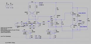
OK a bit of a mash up of unequal items. R10 and R11 should be the same value, make them both 10k. Add capacitor to the input in front of R5, 10uF. R5 should be 1k and C2 1nF. Change R8 to 560 ohms and add a capacitor between it and ground, at least 100uF. Make R6 22-47 ohms. Q6 should be 2n3906. Add .1 to .22 ohm resistors to the emitters of the output transistors. Cross your finger and power it up!
Last edited:
- These were the only 10A transistors in my ltspice library. I am not really using them in the real circuit. I am using sanken audio darlingtons 2SD2390 and 2SB1560 of which I don't have spice models to.
 1 OK that's what I assumed...
2 - I'm under the impression that the 100ohm base resistors are only necessary if there is a emitter follower frequency stability issue or to linearize vbe differences when paralleling output devices. I also assumed since that I was using a single output stage that the emitter resistor wasn't necessary because current sharing wasn't needed like in a parallel output setup. I do think I should put them in to stabilize the bias current.
To a degree they help in single output pairs to stabilise the IQ vs temperature. It gives the base current something to allow small voltage variation to be swamped...
There are some questions about some of your tweaks that I don't understand.
1. Can you explain C6 and R20? I have never seen them used that way. C6 breaks the necessary connection point for R9 which breaks the VBE multiplier. There is 6V of bias in your version causing 2A of bias current in the output stage.
 someone had a crash course in operating LT Spice at 4:30 in the morning to answer your question!!C6 was not intended to break R9 connection - I got in a bit of a "mucking fuddle" attached is the corrected diagram! C6 and R20 help reduce Cdom distortion at higher frequencies if you are careful thd at 1K and 20K can be pretty much the same. I used LTSpice to correct your schematic only, and have just now run many simulations and got to see what it's about.
2. What was wrong with the 4.7k resistors in the current sources? You have changed them to 10k but I don't see the reason.
I doubled them as I took the ground ends to the other supply. this helps keep the amp running correctly at lower voltages and reduce switch on thump.... also prevents DC from flowing in your input circuit ground which I've found helps reduce THD somewhat
3. The 47uf in the feedback path, I will probably add that eventually because it does fix offset problems but as I said in the previous post, it band-aids and covers up the real circuit problems. So once I get the offset in an acceptable range ill put it in.
I'd make that capacitor a non polarised electrolytic as well, I don't encourage the use of polarised in this position.
The original spice circuit was showing dc offset which I got rid of tweaking R1, R2, R6
4. Your C5 5.6pf cap I have not added because the frequency response is currently stable without it and I want to see the true part responses before compensating for safety.
Sometimes you'll find if you take your amp past 100kHz or so the frequency response starts to rise. This is not good and the 5p6 (may need tweaking) helps roll it off sensibly.
5. interestingly the spice I uploaded didn't have any functionality problems but I ran yours and the output clips at 3v. I removed C6 and it fixed the clipping.
fixed - as mentioned above
6. The output base resistors also limit the minimum load impedance. In the simulation the 100R resistors prevent driving below 7 ohms because the transistors cant get enough drive current. My real sanken output transistors have a really high hfe (datasheet say 20000) so the 100 ohms should work in my bench circuit but im not sure they are necessary. I think ill try them as a troubleshooting step though.
Not "stop" so much as "reduce" surely, I did not see what you are expecting into 4 ohms? With darlingtons, you'd make those resistors several orders of magnitude higher, but again, open to tweaking of course taking into account your load requirements....
- Indeed if you're running darlingtons - you could possible get rid of Q5/R15/Q6.......
1 OK that's what I assumed...2 - I'm under the impression that the 100ohm base resistors are only necessary if there is a emitter follower frequency stability issue or to linearize vbe differences when paralleling output devices. I also assumed since that I was using a single output stage that the emitter resistor wasn't necessary because current sharing wasn't needed like in a parallel output setup. I do think I should put them in to stabilize the bias current.
To a degree they help in single output pairs to stabilise the IQ vs temperature. It gives the base current something to allow small voltage variation to be swamped...
There are some questions about some of your tweaks that I don't understand.
1. Can you explain C6 and R20? I have never seen them used that way. C6 breaks the necessary connection point for R9 which breaks the VBE multiplier. There is 6V of bias in your version causing 2A of bias current in the output stage.
someone had a crash course in operating LT Spice at 4:30 in the morning to answer your question!!C6 was not intended to break R9 connection - I got in a bit of a "mucking fuddle" attached is the corrected diagram! C6 and R20 help reduce Cdom distortion at higher frequencies if you are careful thd at 1K and 20K can be pretty much the same. I used LTSpice to correct your schematic only, and have just now run many simulations and got to see what it's about. 2. What was wrong with the 4.7k resistors in the current sources? You have changed them to 10k but I don't see the reason.
I doubled them as I took the ground ends to the other supply. this helps keep the amp running correctly at lower voltages and reduce switch on thump.... also prevents DC from flowing in your input circuit ground which I've found helps reduce THD somewhat
3. The 47uf in the feedback path, I will probably add that eventually because it does fix offset problems but as I said in the previous post, it band-aids and covers up the real circuit problems. So once I get the offset in an acceptable range ill put it in.
I'd make that capacitor a non polarised electrolytic as well, I don't encourage the use of polarised in this position.
The original spice circuit was showing dc offset which I got rid of tweaking R1, R2, R6
4. Your C5 5.6pf cap I have not added because the frequency response is currently stable without it and I want to see the true part responses before compensating for safety.
Sometimes you'll find if you take your amp past 100kHz or so the frequency response starts to rise. This is not good and the 5p6 (may need tweaking) helps roll it off sensibly.
5. interestingly the spice I uploaded didn't have any functionality problems but I ran yours and the output clips at 3v. I removed C6 and it fixed the clipping.
fixed - as mentioned above
6. The output base resistors also limit the minimum load impedance. In the simulation the 100R resistors prevent driving below 7 ohms because the transistors cant get enough drive current. My real sanken output transistors have a really high hfe (datasheet say 20000) so the 100 ohms should work in my bench circuit but im not sure they are necessary. I think ill try them as a troubleshooting step though.
Not "stop" so much as "reduce" surely, I did not see what you are expecting into 4 ohms? With darlingtons, you'd make those resistors several orders of magnitude higher, but again, open to tweaking of course taking into account your load requirements....
- Indeed if you're running darlingtons - you could possible get rid of Q5/R15/Q6.......
Attachments
Last edited:
DC offset in my experience - the matching of Q1 and Q2 is much more important than that of Q13/Q14. Your 10 ohm resistors help, but only drop 10mV which could easily be less than the vbe differences between the two transistors. Increasing to 120 ohms dwarfs these differences and makes them insignificant, giving you no longer need to match Q1/Q2. You may well find you no longer need your offset pot in the emitters of Q13 and 14. I've found resistors at these points can spoil s/n ratio and thd slightly... your call!
Last edited:
Windows has the following information about this file type. This page will help you find software needed to open your file.
.ASC
File Type: Unknown
Description: Windows does not recognize this file type.
You may search the following Web site for related software and information:
.ASC
File Type: Unknown
Description: Windows does not recognize this file type.
You may search the following Web site for related software and information:
Windows has the following information about this file type. This page will help you find software needed to open your file.
.ASC
File Type: Unknown
Description: Windows does not recognize this file type.
You may search the following Web site for related software and information:
download and install ......
Linear Technology - Design Simulation and Device Models
... and all shall be revealed......
Member
Joined 2009
Paid Member
Some general points:
Not everyone uses or wants to use LTspice, so not everyone is capable of reading ASC files. How about attaching a screenshot of the schematic (as another user did in this thread)?
Regarding the circuit:
1) Output transistors need emitter resistors! There are curcumstances where they can be avoided but this is not one of them. Without that, the amp will be extremely thermally unstable. Re acts as a form of local feedback that reduces thermal dependency of Ic - the input voltage to the base required is then Vbe + Vre, and since Vre increases if Vbe decreases and causes higher current to flow, the net variation of the sum is reduced.
2) 100 ohm base resistors are NOT used to improve current sharing. Under normal circumstances the base currents into the outpur stage are so small that the voltage drop on 100 ohms is negligible even in terms of the exponential Vbe-Ic law. The emitter resistors are used to improve current sharing by dropping a voltage higher than than the Vbe variation between parallel transistors. THe 100 ohm base resistors are called 'base stoppers' and prevent local oscillation especially when the output stage is driven by a low impedance source. In your case it's not but you use fairly fast transistors so some form of a base stopper might be required, though I'd expect the amp to work without them.
3) If you are using sanken darlingtons, then WHY are you drawing the schematic as if ut was something entirely different? The whole point of simulation is to make your circuit as close to the actual one as possible. Garbage in - garbage out. It only takes 2 minutes to google what's inside your Darlington transistor, and copy that into your schematic - and it sure isn't what's in the schematic now. It also takes about 2 minutes to google 2N3055 and D45H11 and decide which one resembles what you have more - that would be the D45H11. If it is in the library, it's complement the D44H11 will be there too. For the front transistor in the darlington pack you might consider BD139/140 or BC639/640, or MJE340/350 etc. 1A, 50-100MHz. Voltages are not so important as LTspice does not check maximums by default.
4) Input stage: the differential pair is WAY too degenerated by 250 ohms in the emitters, but the current mirror is under-degenerated, at least 47 ohms should be in the emitters. Quick rule of thumb, emitter resistors in the current mirror = 2x emitter resistors in the diff pair. Adjust for best results later. Input diff base currents come from the input and from the output respectively. In a simulator all transistors of the same type are precisely equal and therefore perfectly matched. Not so in the real worls but emitter resistors will help matters. The point is, base currents produce voltage drops in the input and feedback resistors, and the input diff pair will gladly amplify their difference just as if it was an input signal. Hence the DC offset. THe diff inputs should see the same impedance on both sides for minimum offset.
In your cese there is a signal source (ideal) which has a zero internal impedance. Will this be so in the real world? When testing, check if offset changes when the input is shorted to ground! Bipolar input amplifiers tend to have a capacitor on the input to isolate source impedance at DC from the amp, in order for it not to change the DC offset on the output. Also, the feedbak network ioften includes a DC blocking cap which increases feedback as frequency reduces to near DC, to the point where the total gain of the amp reduces to 1 at DC. This also makes the gain 1 for any DC offset, hence reduces DC offset further.
5) Know your simulator. Again, circuits should resemble reality as much as possible. That being said, sometimes you want to investigate circuit behavior under ideal circumstances. For instance, your simulated amp has decoupling capacitors (2x 2.2uF) on each rail. However, it is powered from two IDEAL voltage sources. Which have zero internal impedance. So, any impedance (such as your capacitors) in parallel with zero equals... and does what? Similarly, caps in the simulator are ideal, so reduce the load on the simulator by using a single component instead of two in parallel. Not a great consideration in your particular case, but just good common sense practice when doing sims. The only case where one might not follow that rule is if you also ose the simulator to keep your bill of materials for a project, however this is not really what they are for.
- Status
- This old topic is closed. If you want to reopen this topic, contact a moderator using the "Report Post" button.
- Home
- Amplifiers
- Solid State
- Need help getting this basic DIY amp up and running (DC offset Problems)