Hi!
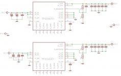
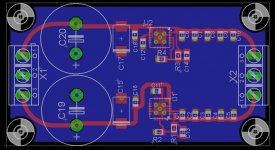
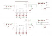
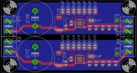
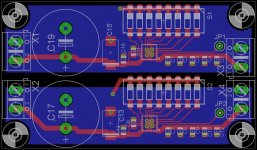
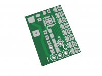
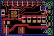
So I was checking web to see if there are any new LDO regulators that have low noise output, so I came across TPS7A4701 and TPS7A3301. Both regulators have approximately same specs and are capable of giving 1A output, input voltage is up to +/-36V and maximum output voltage is +/- 33V, which is ideal for preamplifiers, DACs, headphone amps and similar devices. I designed eagle library and PCB which is now in size 66.5mm x 36.3mm. I would like to know what do you think about PCB layout and I would like to know how much should those pads on QFN package need to look out of it to make good solder joints.
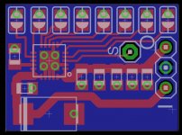
As you will see on the bottom is GND plane to provide enough large area to dispense heat and even maybe to attach it to the heatsink.
Regards,
Ales
So I was checking web to see if there are any new LDO regulators that have low noise output, so I came across TPS7A4701 and TPS7A3301. Both regulators have approximately same specs and are capable of giving 1A output, input voltage is up to +/-36V and maximum output voltage is +/- 33V, which is ideal for preamplifiers, DACs, headphone amps and similar devices. I designed eagle library and PCB which is now in size 66.5mm x 36.3mm. I would like to know what do you think about PCB layout and I would like to know how much should those pads on QFN package need to look out of it to make good solder joints.
As you will see on the bottom is GND plane to provide enough large area to dispense heat and even maybe to attach it to the heatsink.
Regards,
Ales
Attachments
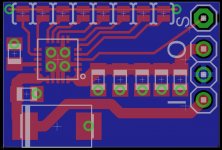
R2, R4 daj čimbližje izhodu, kjer je priklopljeno breme. Več na ZS, da ne smetim.
R2, R4 put closer to the output, where load is connected. More on PM.
Dont put R2,R4 closer to the output cause you dont know what additional parasite inductance will bring into error amplifier circuit. (or make an alternative connections, so you can choice letter on)
About QFN pads, get the size from data sheet. Make it a bit bigger for your own safety.
Devilsdance7775 said:Dont put R2,R4 closer to the output cause you dont know what additional parasite inductance will bring into error amplifier circuit. (or make an alternative connections, so you can choice letter on)
Really?

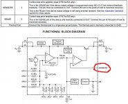
Longer trace won't introduce any additional parasitic inductance into error amp. Longer trace will only introduce negligible voltage output error (inductive reactance * 350nA current through FB pin), since R2 is sense node, similar like ADJ pin on LM317 regulator.
Mixing Sense/Force track is bad, if you want low noise. Running force current through sense track will introduce voltage noise, for example, running 100mA through 1miliOhm will give you 100uV.
Look into datasheet, Figure 23. Or check excellent Walt Jung papers. Or Salas shunt regulator thread. Or Peufeu's explanation here.
Really?
Longer trace won't introduce any additional parasitic inductance into error amp. Longer trace will only introduce negligible voltage output error (inductive reactance * 350nA current through FB pin), since R2 is sense node, similar like ADJ pin on LM317 regulator.
Mixing Sense/Force track is bad, if you want low noise. Running force current through sense track will introduce voltage noise, for example, running 100mA through 1miliOhm will give you 100uV.
Look into datasheet, Figure 23. Or check excellent Walt Jung papers. Or Salas shunt regulator thread. Or Peufeu's explanation here.
trust no one but me
 do not move these resistors
Wery good... Can you also made some 3pin mini regulator for hifi gear replacement.
Like this one...
I will design one, with programmable output and with sensing circuit, to use it for 3.3V and 5V, +/-12V will be using same scheme as in first post.
R2, R4 daj čimbližje izhodu, kjer je priklopljeno breme. Več na ZS, da ne smetim.
R2, R4 put closer to the output, where load is connected. More on PM.
Looking at TPS7A4701 EVM those two resistors are as close a possible to the regulator. Also current through the FB is 35nA when having R2 value of 10kohm.
trust no one but me
As I see it I will have to trust measurements and nobody else
Looks good Ales - Definitely something I could use.
If there will be good results than I might make some ready build boards.
Stay tuned
Best Regards,
Ales
To make this "sense pin" useful, then it would be better to use two TPS7A4701. If using sense only on positive line and no sense pin on negative, then the circuit wouldn't have any benefit with it, as negative side would be, I expect, noisier.
BR,
Ales
p.s. Hopefully I will post new PCB this evening.
BR,
Ales
p.s. Hopefully I will post new PCB this evening.
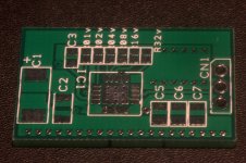
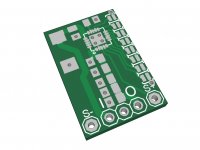
Something like this maybe? Dimensions are 21.5mmx15.80mm, I could maybe squeeze it a little bit if using smaller solder jumpers.
BR,
Ales
Dimensions are 21.5mmx15.80mm, I could maybe squeeze it a little bit if using smaller solder jumpers. BR,
Ales
Attachments
Last edited:
Something like thisSomething like this maybe?
BR,
Ales
Attachments
Hello,
Second version of smal 3pin regulator is nice.
For big version i suggest complete regulator with diodes... make no sense half of big regulator to use. Dip switches is very good idea. Maybe do it so that can be brakable in more pieces if we use just one regulator. So AC input 4 smd schotky diodes big capacitor or even CRC and combination. Maybe at the output resistor diode combination for eye checkind that regulator is working and for empty the regulator if it is not connected to any load.
Odlično, sporoči kdaj bo izdelava in se priključujem nakupu, ker so doma v predalu TPS-ji neuporabni
l.p.
Hi, you mentioned you will design this regulator for 3.3, 5 and 12V. This would be excellent to supply a PC. What are the max current capabilities of your design? Is it possible to have a 1,35V supply as well?
Hi,
regulator has programmable voltage output, so setting 3.3V 5V and 12V isn't a problem. Current capability is 1A. No, 1.35V isn't possible to have, but 1.4V is.
BR,
Ales
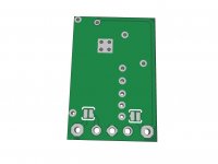
Final version of 3pin regulator?
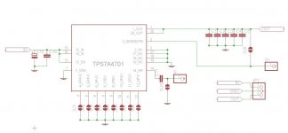
I believe this is the final version of 3pin regulator. Dimensions are 21.5mm*14.45mm, and this is really small. I added sense pins for + and -, this would improve quality of regulator, but if not needed they can be shorted with solder jumpers. (BTW I got hint via PM for sense pins). Through the weekend I will also try to complete PCB for dual voltage, and in the beginning of the next week, send gerbers for PCB production.
BR,
Ales
I believe this is the final version of 3pin regulator. Dimensions are 21.5mm*14.45mm, and this is really small
. I added sense pins for + and -, this would improve quality of regulator, but if not needed they can be shorted with solder jumpers. (BTW I got hint via PM for sense pins). Through the weekend I will also try to complete PCB for dual voltage, and in the beginning of the next week, send gerbers for PCB production. BR,
Ales
Attachments
can the input and output caps be tantalum KEMET make?
Generally its said Tantalums are better than ceramics or may be equivalent to ceramic
Invalid Request
Generally its said Tantalums are better than ceramics or may be equivalent to ceramic
Invalid Request
- Status
- This old topic is closed. If you want to reopen this topic, contact a moderator using the "Report Post" button.
- Home
- Amplifiers
- Power Supplies
- Low noise symmetrical PSU TPS7A4701 and TPS7A3301