Hello
I am trying to make my first board and need someone to check if it looks ok.
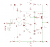
Pcb is for LazyCat's amplifier called vssa (big THANKS for him for schematic).
On my board I didnt put 2 fuses and 2 2,2mF caps (there will be on psu board).
Some small "blocking" caps can be soldered directly to "big" ones on the bottom of board.
Transistors are fitted on the bottom of board - one on top the other one.
The top layout has only 3 connections - which can be replaced with some wire in case of single pcb layout.
If someone can have a look what I need to correct please ?
THX
I am trying to make my first board and need someone to check if it looks ok.
Pcb is for LazyCat's amplifier called vssa (big THANKS for him for schematic).
On my board I didnt put 2 fuses and 2 2,2mF caps (there will be on psu board).
Some small "blocking" caps can be soldered directly to "big" ones on the bottom of board.
Transistors are fitted on the bottom of board - one on top the other one.
The top layout has only 3 connections - which can be replaced with some wire in case of single pcb layout.
If someone can have a look what I need to correct please ?
THX
Attachments
In the ultra performance amp thread active at the moment there is a pcb by Alex.
Look at how he does the power leads next to the power earth and the input far away. His work is always very tidy, you could search his other posts and learn a lot.
I had a chat with Harry Dymond and others about layout in thread "Has anyone seen this..." You could search for that and it may help.
Best wishes
David
Thanks very much !! I will try to find those posts.
It starts here has-anyone-seen-front-end-before-80.html#post3151499
He has an artist's eye for an attractive layout as well as a functional one.I looked at Alex work
Best wishes
David
Last edited:
Bias for vas and output devices is the same as vssa 1.4 oryginally posted by the lazycat, so it schould work corretly.
Hi borys
Looks you were too fast at VSSA sch redrawing, this bias controller will not work. Please check again and be careful at 1:1 inspection.

First thing I noticed,
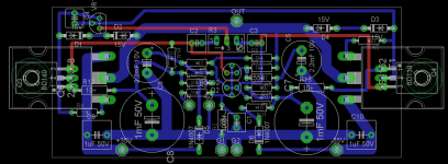
is that you are using two sides, so double up on the high current traces on both top & bottom layer where you can and make it the highest priority nets to routed first.
This reduces the track Z = lower temp rise & adds extra strength to the PTH.
The ground returns, for the o/p transistor filter caps and zobel network should be on separate leads back to the common point ground.
Design, doubling up on O/P devices is always a good idea to improve performance, hands down.
Actually when I look at the placement some more, the gate drive length is way to long for my liking. i'd put the o/p FETs side by side.
Rick
Did you even glance at the datasheet for the output transistors? If you had, you would have noticed that they have Zener protection diodes built in. Lateral fets should be bias around 100mA or so, and this can be done by a simple pot between the gates.(parallel C4) Source ballast resistors are a good idea even for lateral fets, it helps reduce the % difference in Gm for large and small signals, somewhat. It appears the IPS and VAS bias is dependent on B+/B-. This might fluctuate under load and rail sag. Perhaps a CCS would be better instead of R16/R17? Looks like a job for a J-fet. If I were you I would construct the circuit on a breadboard and get it right with proper compensation before drawing the PCB. You may find bugs in the real circuit that must be exterminated. As Rick points out above, there are some design issues with the PCB.
It appears the IPS and VAS bias is dependent on B+/B-. This might fluctuate under load and rail sag. Perhaps a CCS would be better instead of R16/R17? Looks like a job for a J-fet. If I were you I would construct the circuit on a breadboard and get it right with proper compensation before drawing the PCB. You may find bugs in the real circuit that must be exterminated. As Rick points out above, there are some design issues with the PCB.
Last edited:
CBS240 I agree, since this sch comes from PeeCeeBee thread and is derived from VSSA's sch which is different kind of animal, some things here should be changed, yes.
ALF mosfet used in VSSA doesn't have integrated protection zeners, so here can be omitted. Bias trimmer is not recommended here since VAS BJTs are on the same temp as an output laterals, so TL431 serves to stabilize bias voltage without tempco influence of the main heatsink. Source resistors are not necessary for ALFs, here they can be implemented. Input bias CCSs are in VSSA, here also recommended but since this sch comes from PeeCeeBee thread, there CCSs were omited. Compensation in relation with PCB layout is also another story.
ALF mosfet used in VSSA doesn't have integrated protection zeners, so here can be omitted. Bias trimmer is not recommended here since VAS BJTs are on the same temp as an output laterals, so TL431 serves to stabilize bias voltage without tempco influence of the main heatsink. Source resistors are not necessary for ALFs, here they can be implemented. Input bias CCSs are in VSSA, here also recommended but since this sch comes from PeeCeeBee thread, there CCSs were omited. Compensation in relation with PCB layout is also another story.
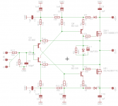
I draw the schematic again (hope correct this time), and have some questions:
1.Output tranies resistors 0,22r must be on the sources side or I can fitt them on drains side ?
2.For VAS bias thermal stability in this circuit would be beter to keep them on separate heatsink or main heatsink with laterals?
As cbs240 sugested I am getting breadboard for tests but must start with somethink anyway.
Sory If my questions are stupid but before I learn somethink I have to ask stupid questions.
THX
Attachments
- Status
- This old topic is closed. If you want to reopen this topic, contact a moderator using the "Report Post" button.
- Home
- Amplifiers
- Solid State
- My first PCB - some help needed