Hi All,
I am desigining a DIY DAC and I want to make it as modular as possible by physically separating it into 4 PCB's.
-USB/Digital In
-DAC
-I/V Stage
-PSU
My main concern is with the return paths of the Signals that come in and out of the USB/Digital IN, DAC, and IV stages. The signal lines include I2S wires that I need to run with a proper return path.
As you can see by the diagram that I am including I am concerned that I might be creating ground loops..... or AM I?
I want to provide a clean parallel return path for all of my board to board signal lines. Some of those signal lines are I2S.
If I pay attention to the layout and keep PSU lines away from the singal lines, the return paths should not create any unwanted ground loops, correct?
Thanks for your input guys
Attachments
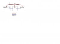
The diagram clearly shows three ground loops and in practice you'll have more---the output of the IV stage goes somewhere, no? Remember that current follows the path of least impedance and that kHz or MHz signals ultimately turn into low fequency mains related ripple in the supply somewhere. So while, say, I2S edges will follow the path of least inductance they inevitably lead to low frequency mains slosh that will happily follow the path of least resistance that shuts some current into any parallel ground connection. You can try to drive the resulting ground balance to zero but generally high end audio performance requirements are such that it's more effective to structure the circuit topology for good CMRR.
See, oh, the couple pages of discussion starting here for more or search my posts; I tend to comment on things like this rather often.
See, oh, the couple pages of discussion starting here for more or search my posts; I tend to comment on things like this rather often.
See, oh, the couple pages of discussion starting here for more or search my posts; I tend to comment on things like this rather often.
twest thanks for the incite! I think I will stick with my wiring topology since there is no other real way to do this really. When I wire "over the air" from board to board I will make a twisted pair so the signal will have a good return path to the source weather that is USB receiver to DAC PCB. As long as my layout is good and components are physically separated I believe that ground loops will be avoided. Need to make sure that there is a path of least resistance for the return signal and not route like spaghetti hehehe
The expert onitems such as this is Henry W. Ott:
Henry Ott Consultants
Electromagnetic Compatibility Consulting and Training
home page
Speed, I have been to his website before and I have read some of his papers before! Thanks for the reminder! That is where I thin that I will be ok wiring between boards and will avoid ground loops as long as I keep my layout clean and avoid crisscrossing signals and routing randomly trough broken ground planes
")
This paper by Henry Ott is great! I need to re-read it! Thanks for reminding me!
http://www.hottconsultants.com/pdf_files/june2001pcd_mixedsignal.pdf
- Status
- This old topic is closed. If you want to reopen this topic, contact a moderator using the "Report Post" button.