Vertical Fet Output Stage...that actually WORKS!
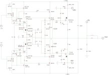
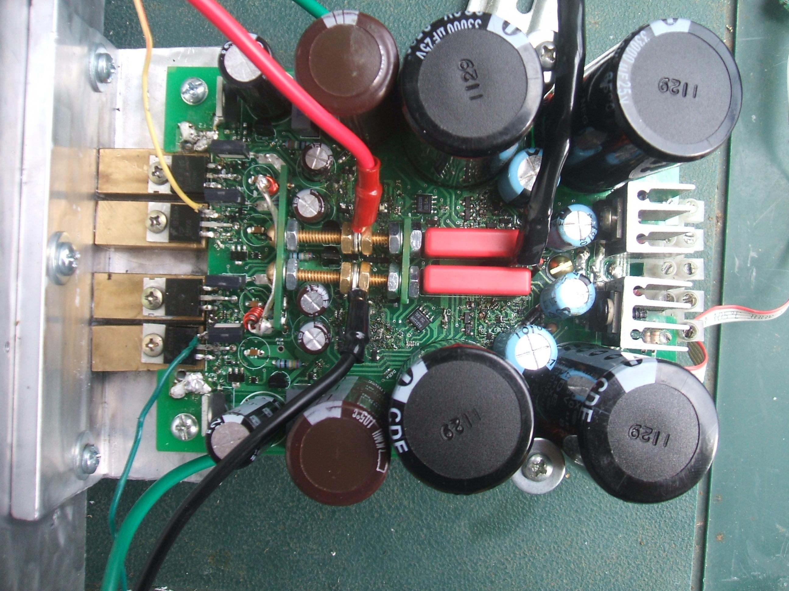
Here is a little circuit you guys can play with. This is the latest output stage I am using. It is a source follower with an advanced HEC gate drive circuit. Here is some reference papers on HEC, it is nothing new. Hawksford HEC, Bob's EC paper Notice the frequency compensation is set roughly about 3X higher than the example in Bob's paper. The output transistors are of course not exactly equal, but this is really the experiment. How much garbage can the EC circuit mitigate? Evidently quite alot. The output is very accurate. You don't get the extra heavy bass or fuzzy highs that these components are known for. The output fets are planer stripe vertical mosfets directly mounted onto a chunk of brass that acts as an extra large heat slug, effectivly making them much larger transistors and very robust. (example of OT mounting)I would normally use FQP50N06/FQP47P06 because they have a more similar Gm, but the price on those has gone up. They now cost ~$2 each. FQP33N10/FQP27P06 only cost $1 each. Don't underestimate these components because of the TO-220 package, I cranked 100Wrms into a 2R2 resistor with just one pair and they did not fail. 65Wrms @ 4R speaker is no problem for this output stage. The error amplifiers, with the -*-, are to be mounted so as they are in contact with the drain pin of the output transistors for thermal compensation. Basically, in order to correct for the distortion created by these output devices, the error signal (the signal representing the inverse of the output transistor transfer) is added to the audio signal and amplified to drive the gates of the mosfets. Since the transfer curve of vertical mosfets is significantly exponential, the error signal must be logarithmic in nature. This means the slope of the tangent on this curve becomes very steep in the region where the mosfet is conducting little current, around crossover, indicating very high order frequency information. The slope of the error signal at this region is an indication of this RF information. In order to create the frequency range to optimize error correction of these output devices I use high frequency RF transistors. Because these transistors are limited in Vceo ~15V, they are cascode by ordinary small signal devices in order to create an 'envelope' for them to operate within. Also the whole driver envelope is effectively cascode by the bootstrap. This allows me to use small signal devices and still have the same (or better) operation. I'l post some waveforms later. The great thing about this circuit is it requires a constant current of ~2uA to drive. It does not matter if the output is conducting 10A or 10mA, the load on the VAS is always constant, as if you attached a small 2uA CCS to the output of the VAS.
Always having fun defying the audiophool community by creating a most superb power amplifier using components they say "those are switching transistors and can't be used for Hi-Fi linear audio." This is complete non-sense, and not just my opinion.
Datasheets:
2SC6026/2SA2154
BFR92AW/BFT93W
BFQ19/BFQ149
MMBT5179
H81
FQP33N10/FQP27P06
Here is a little circuit you guys can play with. This is the latest output stage I am using. It is a source follower with an advanced HEC gate drive circuit. Here is some reference papers on HEC, it is nothing new. Hawksford HEC, Bob's EC paper Notice the frequency compensation is set roughly about 3X higher than the example in Bob's paper. The output transistors are of course not exactly equal, but this is really the experiment. How much garbage can the EC circuit mitigate? Evidently quite alot.
The output is very accurate. You don't get the extra heavy bass or fuzzy highs that these components are known for. The output fets are planer stripe vertical mosfets directly mounted onto a chunk of brass that acts as an extra large heat slug, effectivly making them much larger transistors and very robust. (example of OT mounting)I would normally use FQP50N06/FQP47P06 because they have a more similar Gm, but the price on those has gone up. They now cost ~$2 each. FQP33N10/FQP27P06 only cost $1 each. Don't underestimate these components because of the TO-220 package, I cranked 100Wrms into a 2R2 resistor with just one pair and they did not fail. 65Wrms @ 4R speaker is no problem for this output stage. The error amplifiers, with the -*-, are to be mounted so as they are in contact with the drain pin of the output transistors for thermal compensation. Basically, in order to correct for the distortion created by these output devices, the error signal (the signal representing the inverse of the output transistor transfer) is added to the audio signal and amplified to drive the gates of the mosfets. Since the transfer curve of vertical mosfets is significantly exponential, the error signal must be logarithmic in nature. This means the slope of the tangent on this curve becomes very steep in the region where the mosfet is conducting little current, around crossover, indicating very high order frequency information. The slope of the error signal at this region is an indication of this RF information. In order to create the frequency range to optimize error correction of these output devices I use high frequency RF transistors. Because these transistors are limited in Vceo ~15V, they are cascode by ordinary small signal devices in order to create an 'envelope' for them to operate within. Also the whole driver envelope is effectively cascode by the bootstrap. This allows me to use small signal devices and still have the same (or better) operation. I'l post some waveforms later. The great thing about this circuit is it requires a constant current of ~2uA to drive. It does not matter if the output is conducting 10A or 10mA, the load on the VAS is always constant, as if you attached a small 2uA CCS to the output of the VAS. Always having fun defying the audiophool community by creating a most superb power amplifier using components they say "those are switching transistors and can't be used for Hi-Fi linear audio." This is complete non-sense, and not just my opinion.
Datasheets:
2SC6026/2SA2154
BFR92AW/BFT93W
BFQ19/BFQ149
MMBT5179
H81
FQP33N10/FQP27P06
Attachments
Last edited:
The feedback loop adjusts for any unlinearities.
Only until the relatively limited global loop BW limit is reached. One of the reasons for Dr Cherry's work with nested loops.
All of that HF stuff that passes through the input stage can affect it's performance in a negative way. This circuit is a nested feedback/feedforward circuit, that is if you include it within the closed loop of the IPS and VAS. This is optional.
Last edited:
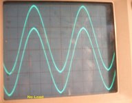
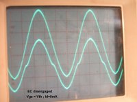
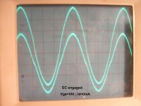
Here, the output stage follower circuit with the EC amplifier is NOT within a global loop. The only global loop is from the output to the DC servo of the amp, but as far as the audio signal is concerned the output stage is purely a follower, output current buffer. I drew into the PCB a single connection for a jumper to attach the error amplifier input to the output. This allows me to easily switch the error correction on or off. The first photo is 1KHz, 3Vp with no load attached. The gate drive is the top waveform and the output is the bottom. The output devices are bias right at Vth, 0V appears across the source resistors. As one would expect the output appears identical to the gate drive. The second photo shows the output with the EC switched off driving 2R, so 1.5Ap. It is clear there is a significant period of time where neither output transistor is conducting, while the gate drive signal stays the same. The same conditions exist in the third photo except the EC is active. Although there is still a small bit of crossover distortion, it is much less pronounced, considering these type of outputs are bias in Class B. The slope and magnitude of the gate drive signal changes to try and fill in the difference. With bias more than 30mA or so, the crossover is not noticeable with the EC switched on. Id >100mA is really about where you would want to bias, I just wanted to show that the action of the EC is sound and that it really does eliminate a huge amount of distortion that would otherwise find itself with in the IPS and VAS, clearly not where it belongs.
Attachments
I found in my experiments that the VAS local feedback loop was vital to stability.
100pf to 270pf fixed any oscillation on the outputs.
The value of compensation cap depends on the impedance of the VAS and the amount of linear OLG & PM. Often this is a function of the load on the VAS, which is variable with the output load assuming a typical EF driver stage. This circuit allows you to place a more constant load on the VAS so as not to have to over dampen the IPS/VAS just to prevent the occasional oscillation burst. Local compensation of the Mosfets is vital to stability, or you can over dampen the circuit and trade bandwidth for stability. Not a good trade IMO.

- Status
- This old topic is closed. If you want to reopen this topic, contact a moderator using the "Report Post" button.