Hi. I've recently began looking into the different classes of amplifiers and I've made a class A amp as well as a class B push-pull amp (I believe), but I'm struggling to see the differences between them.
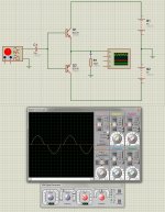
I believe that when an amp is operated in class A, current will flow through the transistors even when there is no output. This eliminates crossover distortion which is why this design has been popular among the audiophools, right? What about this push-pull design:
Am I right to say that this is a class B push-pull amp and that a clean "Class B" amp is one where only half the waveform is amplified?
If the above schematic is a class B, what is a class AB then? I've seen someone saying that a class AB amp is an amp that has it's input transistors biased to a certain voltage so that the transistors are on up to a certain output level making it class A for the first few watts and then class B for the rest. This sounds reasonable, but isn't there a theoretical efficiency of class AB amps of 78.5% or something like that? Surely the efficiency would be worse when it's operated in class A and then much better when it's operated in class B? And the "avarage" efficiency throughout the whole output power range would then depend on how the transistors are biased? Let's say it's biased so that it's operated in class A for the first mW and then class B up to 50W, that would make in class B in practice, but technically a class AB amplifier, no?
I managed to calculate the theoretical efficiency of a class A amp to 25% which I'm happy about, but I can't get the same result for the amp in the image I posted. If the amplifier is ran at full power, at the point of clipping, won't then the voltage and current through the transistors be the same as the voltage and current through the load? When the voltage across the load is equal the the supply voltage, the voltage across one transistor is 0V. When the voltage across the load is 0V, the voltage across the transistor is equal to the supply voltage. I can't understand how this doesn't make the efficiency 50% as the load power is equal to the transistor power (when the power from both transistor is added together that is).
I also have a question about crossover distortion. When I try to simulate the class B push-pull amp that I linked, I clearly saw the crossover distortion, but when I made the amp (with BJT's) and scoped the output, I saw absolutely no crossover distortion and I couldn't hear any difference either when listening to a sine wave either. On wikipedia it says that because of this crossover distortion, class B push-pull amps aren't that viable for audio, but when using BJT's with a threshold voltage of ~0.7V and an op-amp input stage with a high slew rate, can this really be audible?
And about the difference between a class AB design (with it's transistors biased) and class A when it comes to crossover distortion. If the transistors are biased above the threshold voltage, I can't understand how there can be any crossover distortion at all regardless of output power. Even when the output power is high enough to completely turn off one of the transistors, that transistor will still start to turn on before the load voltage reaches 0V and begins to rise (or lower) to the other half of the sine wave, so there is no need for an input stage to 'overcome' this threshold voltage. What is then the point of a pure class A design?
Another question I have is about my newly bought Rigol DS1052E scope. It has a TTL function which I was happy about, I could finally see how much distortion my amps were having It didn't quite turn out that way since every amp I make has no visible distortion The other harmonics are down at the noise level and they become visible at the same moment I can see the sine wave beginning to clip and at the same moment I can faintly hear the sine wave becoming a little distorted. So I guess the question is, how much distortion is actually there when a sine wave looks more or less perfect on the little screen of an oscilloscope?
I didn't plan on asking this many questions, I sort of got carried away I appreciate any help
I believe that when an amp is operated in class A, current will flow through the transistors even when there is no output. This eliminates crossover distortion which is why this design has been popular among the audiophools, right? What about this push-pull design:
An externally hosted image should be here but it was not working when we last tested it.
Am I right to say that this is a class B push-pull amp and that a clean "Class B" amp is one where only half the waveform is amplified?
If the above schematic is a class B, what is a class AB then? I've seen someone saying that a class AB amp is an amp that has it's input transistors biased to a certain voltage so that the transistors are on up to a certain output level making it class A for the first few watts and then class B for the rest. This sounds reasonable, but isn't there a theoretical efficiency of class AB amps of 78.5% or something like that? Surely the efficiency would be worse when it's operated in class A and then much better when it's operated in class B? And the "avarage" efficiency throughout the whole output power range would then depend on how the transistors are biased? Let's say it's biased so that it's operated in class A for the first mW and then class B up to 50W, that would make in class B in practice, but technically a class AB amplifier, no?
I managed to calculate the theoretical efficiency of a class A amp to 25% which I'm happy about, but I can't get the same result for the amp in the image I posted. If the amplifier is ran at full power, at the point of clipping, won't then the voltage and current through the transistors be the same as the voltage and current through the load? When the voltage across the load is equal the the supply voltage, the voltage across one transistor is 0V. When the voltage across the load is 0V, the voltage across the transistor is equal to the supply voltage. I can't understand how this doesn't make the efficiency 50% as the load power is equal to the transistor power (when the power from both transistor is added together that is).
I also have a question about crossover distortion. When I try to simulate the class B push-pull amp that I linked, I clearly saw the crossover distortion, but when I made the amp (with BJT's) and scoped the output, I saw absolutely no crossover distortion and I couldn't hear any difference either when listening to a sine wave either. On wikipedia it says that because of this crossover distortion, class B push-pull amps aren't that viable for audio, but when using BJT's with a threshold voltage of ~0.7V and an op-amp input stage with a high slew rate, can this really be audible?
And about the difference between a class AB design (with it's transistors biased) and class A when it comes to crossover distortion. If the transistors are biased above the threshold voltage, I can't understand how there can be any crossover distortion at all regardless of output power. Even when the output power is high enough to completely turn off one of the transistors, that transistor will still start to turn on before the load voltage reaches 0V and begins to rise (or lower) to the other half of the sine wave, so there is no need for an input stage to 'overcome' this threshold voltage. What is then the point of a pure class A design?
Another question I have is about my newly bought Rigol DS1052E scope. It has a TTL function which I was happy about, I could finally see how much distortion my amps were having
It didn't quite turn out that way since every amp I make has no visible distortion The other harmonics are down at the noise level and they become visible at the same moment I can see the sine wave beginning to clip and at the same moment I can faintly hear the sine wave becoming a little distorted. So I guess the question is, how much distortion is actually there when a sine wave looks more or less perfect on the little screen of an oscilloscope?I didn't plan on asking this many questions, I sort of got carried away
I appreciate any help It's time to read some educational articles rather than picking away with necessarily brief forum replies.
Start with this article and cover the different classes in following articles. There is plenty of relevant reading there.
Start with this article and cover the different classes in following articles. There is plenty of relevant reading there.
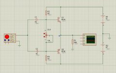
Here are two circuits to sim and build.
The transistors should have small heatsinks, incase
These circuits are intended for QUICK demo,
Don't leave them on, and keep an eye on transistor temperatures !!
They should work when breadboarded.
The second circuit allows to bias the bases abit pushing it into slight class AB.
Turn potentiometer from min to max and observe output waveform on scope.
In slight Class AB the crossover distortion is still there, because there are times that only one transistor is conducting, but it now happens above cuttoff (The zero volt line (gnd)).
This distortion if biased correctly is low enough for a slight Class AB amplifier to be considered HIFI.
Biasing into heavy Class AB isnt necessary for BJTs, others might disagree.
Regards
Attachments
Ian Finch: I have read the guide you posted, I've also read a guide about amplifier efficiency along with several other articles. I posted here because I still don't understand it. I was hoping that someone here might help me understand it by putting it in a different language
Vostro: Yeah, I've seen those circuits before. By "slight class AB", do you then mean an amp where the transistors are biased below the threshold voltage? Because I can see that the more bias you have, the less crossover distortion there will be, what I don't understand is how there can be any crossover distortion at all when the base/gate is biased above the threshold voltage. I can't see any crossover distortion in my simulations atleast.
Vostro: Yeah, I've seen those circuits before. By "slight class AB", do you then mean an amp where the transistors are biased below the threshold voltage? Because I can see that the more bias you have, the less crossover distortion there will be, what I don't understand is how there can be any crossover distortion at all when the base/gate is biased above the threshold voltage. I can't see any crossover distortion in my simulations atleast.
Because when you have both transistor's Gm (transconductance) contributing to the output impedance, and then one turns off so Zout comes from only one transistor. This change in output Z is what gives you the crossover distortion. It is much worse with mosfets because they loose significant % of Gm at lower conducting currents. This is why we use emitter (source) resistors of specific calculated value to minimize the % change in output Z as the output changes from small signals to large signals.
Because when you have both transistor's Gm (transconductance) contributing to the output impedance, and then one turns off so Zout comes from only one transistor. This change in output Z is what gives you the crossover distortion. It is much worse with mosfets because they loose significant % of Gm at lower conducting currents. This is why we use emitter (source) resistors of specific calculated value to minimize the % change in output Z as the output changes from small signals to large signals.
Yes, I can see this being a factor, but with a proper input stage and feedback, how can this still be an issue?
Recall WHY we're "even remotely concerned" about all this class / distortion business!
Class "A" amplifiers have the nominal (no signal, quiescent) conduction of the amplifying elements (transistors, mosfets, fets, tubes, whatever...) set to a point of "half-conduction" - where they can conduct UP to twice as much before signal levels approach the power supply limits, and DOWN to zero in the opposite direction. The "magic" of either output transformers or DC blocking capacitors renders the output purely alternating current, it drives the speakers (or next stages), and life is good.
However, "Class A" power dissipation is HIGHEST when there is no signal! Essentially it is so both by definition and design... just the nature of it. There is no intrinsic distortion apart from the nonlinearity of the amplifying devices, and subtractive (negative) feedback can reduce that further (at the expense of overall gain). Power dissipation though doesn't change. When there is a powerful driving signal, power dissipation in a class "A" barely changes, on the average from quiescent. When powerful, such amplifiers run hot, and stay so indefinitely.
Again, recalling "history", the almost immediate realization of electronic engineers 'way back was ... well, if we pair amplifying devices, and have each of them running only half the cycle, then they could be much closer to cut-off ... which would both save a bundle of power (when quiescent) and double-to-quadruple the amount of output power!
PERFECT for "public address" situations, where POWER is needed to get sound out to the far reaches of a theater, stadium, public or large social event. Distortion - in the chaotic sound-stage of the theatre - hardly matters to a significant degree. So, classic "class B" near-cut-off designs ruled.
Audiophiles since recognized that their quest wasn't for efficiency, or ultimate power, but sweetness of the sound, coupled with speakers far more expensive than would ever be sacrificed on the altar of a public address system. They (we) were searching for musicality, for transparency of tone, of accuracy in reproducing the faint acoustic rarefactions and compressions of air we enjoy so much.
The CLASS-B design you posted first (direct-connected bases and upper-emitter to lower-collector) would work perfectly if the transistors were themselves perfect devices, and not subject to little quantum realities such as 0.7V emitter-base bias. But they are real, physical devices, with real, physical gotchas ... that need to be engineered out for the produced signal to be musically pure of tone, and relatively free from confounding distortions.
Vostro above points out two designs using a synthetic electronic-design "lab bench" program. His left-most design shows an oscilloscope that clearly draws the cross-over gap, the distortion of direct-connected transistors. The second diagram has a more sophisticated design that using resistors and capacitors works to bias the transistors further into their nominal conduction regions, which brings "the gap" toward non-existence. For the most pure signal though, both transistors should be biased WELL into their conduction region. It is the purists approach, and it works. it also consumes more power both on the average, and quiescent.
But ... when one spends thousands and thousands of dollars over years experimenting with building things, and getting better vinyl record players, better speakers, more elaborate preamplifiers and so on ... what's the cost of "wasting" a little more power to just dumb-as-a-rock heat? I say it is cheap. Budget about 15% to 25% of the potential peak power of the amplifier to simple Class A/B heat (or better, just class A heat at a lower power level), and be happy. The sound will be sweet.
GoatGuy
Yes, I can see this being a factor, but with a proper input stage and feedback, how can this still be an issue?
Feedback fixes everything......this is non-sense.
Much of the crossover distortion components are well above the bandwidth of the global loop. Feedback does not get rid of the distortion but merely shifts it to higher order frequencies. Distortion components that are well above the 20KHz audio band limit can affect the sound for sure. You want the feedback to have to 'correct' for as little as possible. IOW, the goal should be that the global loop sees as linear of a transfer through the stages of the amplifier as possible.Feedback fixes everything......this is non-sense. Much of the crossover distortion components are well above the bandwidth of the global loop. This means the feedback does not get rid of the distortion but merely shifts it to higher order frequencies. Distortion components that are well above the 20KHz audio band limit can affect the sound for sure. You want the feedback to have to 'correct' for as little as possible. IOW, the goal should be that the global loop sees as linear of a transfer through the stages of the amplifier as possible.
Could you explain a little further? Where would these higher frequencies come from? About the feedback having to 'correct' for as little as possible, why would this matter? If an op-amp input stage is taken as an example, if then these unlinearities in the power stage are within the limits of the op-amp, shouldn't then the op-amp do it's job and output whatever it needs to output? As long as the op-amp isn't asked to output a voltage it can't output, why would there be distortion? Other than the tiny distortion you would get from an op-amp regardless of the output stage. I can see how a pure class B design will create crossover distortion though as in this design the op-amp is asked to go from 0V to ~0.7V in 0s which is clearly impossible. But taking the class AB design, this threshold voltage doesn't have to be overcome and the same moment the output of the op-amp changes, the output of the power stage will also change.
Feedback reduces distortion. It does not eliminate it. Whether distortion is audible is a matter of argument, hearing ability and personal taste.
Here is what I think feedback is.
Negative feedback amplifier - Wikipedia, the free encyclopedia
I dont know how this works. It reduces gain my the feedback factor and reduces distortion also by the same factor. How useless, why not just turn volume down.
Here is my version of feedback, which i guess doesnt reduce gain and removes all distortion and not just reduce it.
A is input signal
amplifier multiplies by 10
D is distortion
A ---Amp---> 10A+D
A -1/10 D ---Amp---> 10A - D +D = 10A

^ ^
| |
input - (input - 1/10 output)
- (input - 1/10 output) = feedback
Whay say ?
Regarding class A, B and AB
Here is response of transistor
http://www.vlsiinterviewquestions.org/2012/03/26/mos-transistor-current-response/
Class A runs in small middle linear region, so obviously more liner and waste of power
Class B starts from bottom so no output until it input reaches 0.7v or something threshold, Class AB get rid of this 0.7 threshold problem by running at aprox 0.7 transistor even in idle.
Also notice Class B, Class AB uses more region of the response curve and as you can see the curve is Not liner.
extra info Class D operates out of all this liner region and runs in saturation region.
Last edited:
Could you explain a little further? Where would these higher frequencies come from? About the feedback having to 'correct' for as little as possible, why would this matter? If an op-amp input stage is taken as an example, if then these unlinearities in the power stage are within the limits of the op-amp, shouldn't then the op-amp do it's job and output whatever it needs to output? As long as the op-amp isn't asked to output a voltage it can't output, why would there be distortion? Other than the tiny distortion you would get from an op-amp regardless of the output stage. I can see how a pure class B design will create crossover distortion though as in this design the op-amp is asked to go from 0V to ~0.7V in 0s which is clearly impossible. But taking the class AB design, this threshold voltage doesn't have to be overcome and the same moment the output of the op-amp changes, the output of the power stage will also change.
Propigation delay is one factor. Every stage adds just a little bit of propigation delay to the system. Capacitances within the circuit and components do not charge instantly. The negative feedback loop is always trying to play catch up. It's not about asking the op-amp to provide an output voltage it isn't capable, in your example above, it is asking the op-amp or IPS+VAS to output a slew rate beyond it's limit, thus leaving the distortion from the output stage in the output signal. Although class AB is bias above cut-off, as I explained above it is the non-linear change in output Z that is the issue. Class A does not have this problem because Zout is not shared between two devices that are switching on and off. Here is an example of crossover distortion being seen dispite being class AB bias. The experiment is with mosfets dealing with error correction, a more sophisticated local nested feedback/feedforward circuit showing where they suffer a drop in Gm at the crossover region. The top waveform is the output. The bottom waveform is the error signal, or the inverse of the distortion products created, and clearly shows the required slew to drive the devices to linear output at different bias levels. This gives validity to Mr. Cherry's admiration of using nested feedback loops.
Last edited:
You are conflating two different things: propagation delay and filtering caused by capacitance. In almost any audio amplifier propagation delay can be completely ignored when considering distortion or loop stability. Filtering caused by capacitance is an important issue which complicates things.CBS240 said:Propigation delay is one factor. Every stage adds just a little bit of propigation delay to the system. Capacitances within the circuit and components do not charge instantly.
However, filtering does not cause re-entrant distortion. This would still occur with an infinite bandwidth but distorting amplifier. In fact, it doesn't even need feedback - simple algebra is sufficient arising from a linear component in series with a non-linear component.
You can't subtract off distortion by subtracting off a (supposed) distortionless output. If you have eliminated D in the output (as you claim) then you can't use this perfect output to cancel D in the input, as you have no D left to use. Hence feedback can only reduce distortion, not eliminate it.Amit_112dB said:A ---Amp---> 10A+D
A -1/10 D ---Amp---> 10A - D +D = 10A
^ ^
| |
input - (input - 1/10 output)
- (input - 1/10 output) = feedback
Whay say ?
...cannot subtract off distortion by subtracting off a (supposed) distortionless output.
Actually, I think you missed the point. The author wasn't positing that his algebraic notion was a solution to the problem, but is just an algebraic form that negates it.
It is an interesting notion: that (in theory) one could cobble together an anti-distortion preemphasis network that would compensate without feedback per se for the amplifier's non-linear transfer function. Of course, in the (now) ideal world of having brilliantly simple amplification stages (triodes), the complexity of even a modestly accurate compensation network would dwarf the complexity of the rest of the amplifier.
Agreeing... with you though: in the real world, building conventional amplifiers out of the handful of accepted circuit topologies that we have come to generally agree are among the better ideas, then both local and global compensation feedback serve to remove distortion from the output, and yield amplifiers delivering close to the ideal Output = Amplification * Signal + zero distortion.
And there always must be some distortion on the output in order for the error-amplifiers along the feedback path to have something to react against.
It is for this reason that I'm particularly fond of non-capacitor-bypassed cathode bias resistors in single-ended amplification stages: gain is substantially reduced, even more remarkably linearlized, and the floating cathode (or source, if using FETs, or BJTs) becomes effectively a negative feedback element, that is ultra-local. Not global. Realistically, things such as 12BZ7s are pretty cheap, as are damn-fine newly made JFETs ... so having a few extra amplification stages (at lower per-stage gain) to effect the desired overall gain, is hardly worth gnashing one's teeth over. Especially when all the gain stages are being run in their sweet-spot of gain, amplification and current flow.
GoatGuy
Member
Joined 2009
Paid Member
I am coming to start to believe that the class of amplifier is not as important as the implementation. A very well implemented amplifier of class <insert your favourite letter> will meet your needs. But you won't hear that from commercial vendors (they will peddle their's as the best) and you won't hear it much around here because we're all mad about amplifier design and their minute details and enjoy arguing over them
[Bigun] - you're right. To the point of near-hilarity, I read posts and treatises about the One and True Path [to amplifier nirvana], with staunch advocates of huge triodes, parallel triodes, pentodes, pentodes-as-triodes, cathode followers, gyrators, single ended, AB push-pull designs, H designs, cascode front ends, long-tailed pairs, differential signal paths, symmetric amplification, local feedback, global feedback, phase summing, yada, yada, yada.
In the end - the very most (absurdly) expensive pieces of cabinetry and steampunk valve art - which are described in exquisite (but utterly vapid) terms - inevitably all the designs "err" toward just being hugely overbuilt to become more linear, to offer unfettered output current sources, and to keep frequency response completely beyond question, whether impacting the sound, or not. And, more to the point, the huge coloration-of-tone that is the inevitable consequence of using moving masses to move air, to make sound (AKA "speakers") ... is sidelined in finely written prose. But... its all moving parts.
So long as an amplifier faithfully reproduces the VOLTAGE of the input at the output, in all its little twitches and wiggles, and as long as it can supply whatever CURRENT the speakers in turn demand as their combinations of magnets, windings, couplings, physical responses enact the old 3rd order reactive load equation ... then one can hardly ask more from the amplifier, regardless of how it is designed. The sad truth though is this: most amplifiers only do a "pretty good" job at reproducing the voltage wave, and even fewer do all that good of a job supplying the current resulting from the voltage across the reactive loads. And most that don't do a very good job are push-pull. And most that don't reproduce the overall voltage waveform well are either push-pull, or are using triodes (and transistors) in their raw, uncompensated mode(s). Many a grand design to "cure" or address a perceived ill (such as triode/FET Miller capacitance - a kind of HF negative feedback), will create a whole cartload of other evils in the nominal signal path.
And that's why I laugh.
GoatGuy
GoatGuy said:Actually, I think you missed the point. The author wasn't positing that his algebraic notion was a solution to the problem, but is just an algebraic form that negates it.
Perhaps I misunderstood, but that looks like a claim that his (faulty) algebra indicates removal of all distortion.Amit_112dB said:I dont know how this works. It reduces gain my the feedback factor and reduces distortion also by the same factor. How useless, why not just turn volume down.
Here is my version of feedback, which i guess doesnt reduce gain and removes all distortion and not just reduce it.
Predistortion is used in situations where NFB is difficult, such as linear RF PAs. It is only used in such situations, as elsewhere (such as audio) NFB works better.GoatGuy said:It is an interesting notion: that (in theory) one could cobble together an anti-distortion preemphasis network that would compensate without feedback per se for the amplifier's non-linear transfer function. Of course, in the (now) ideal world of having brilliantly simple amplification stages (triodes), the complexity of even a modestly accurate compensation network would dwarf the complexity of the rest of the amplifier.
- Status
- This old topic is closed. If you want to reopen this topic, contact a moderator using the "Report Post" button.
- Home
- Amplifiers
- Solid State
- Some questions about amplifier classes, distortion and efficiency