Hi everyone,
I have finally powered up my pair of mono block F3's that I started several years ago (good thing I don't do this for a living)") . Between life and all the time I have been sitting and listening to my Aleph-X, I have yet to finish this pair of amps.... until now.
. Between life and all the time I have been sitting and listening to my Aleph-X, I have yet to finish this pair of amps.... until now.
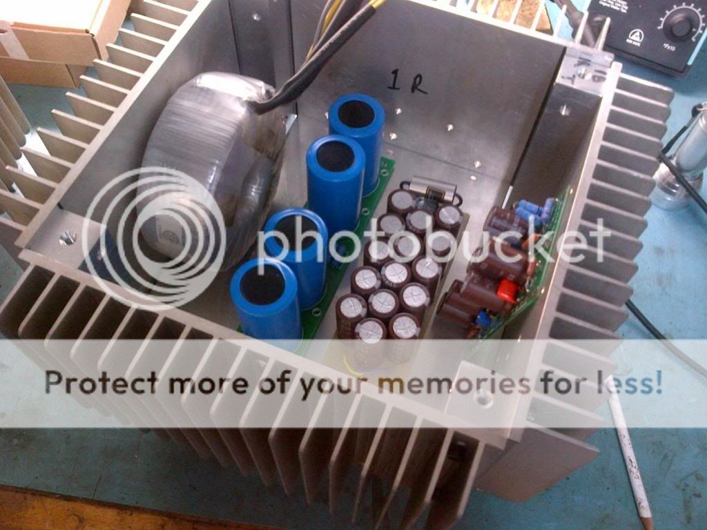
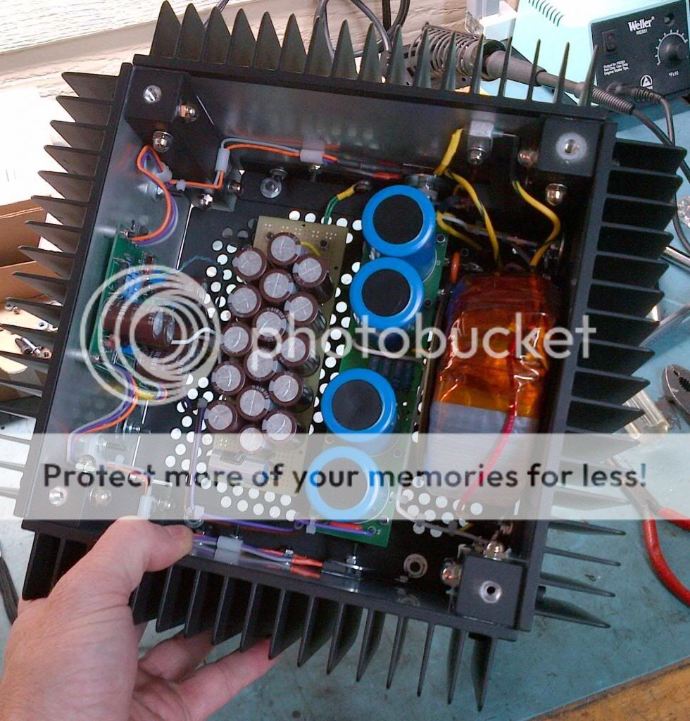
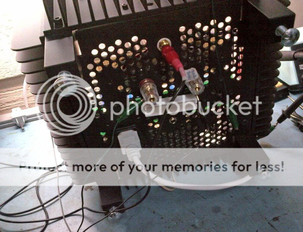
These amps started out originally as ZV9's, but I converted them over to F3's as I completed assembly. The main heat sinks were surplus that I picked up a while ago. The basic construction of these amps was simple due to the machine equipment that I have readily available. These will be placed directly behind my main speakers since the best speaker cable is none at all, so appearance is not a major concern (but they do need to look presentable since they will be in the living room).
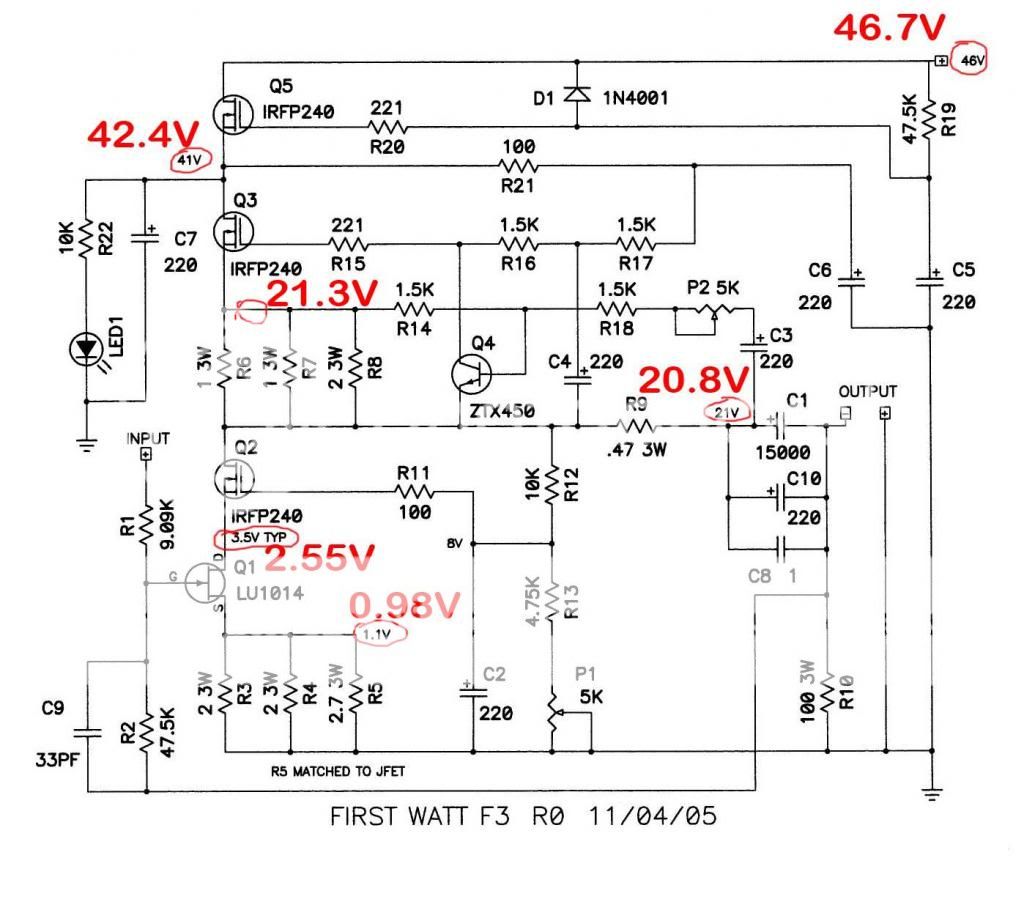
Now that I have both amps up and running, I have a few questions about adjusting them. I have attached a copy of the F3 schematic with the voltages that I am currently measuring ( both amps are basically the same) after an hour or so of warm up time.
The first thing that stands out is that I only have about 1.7 volts across Q1 (not the 2.5V for optimum load line cancellation). Based on the voltages across R6, 7, 8 it looks like I am only biased to about 1.3 amps. This is confirmed by the maximum heat sink temp of 110F near Q2 & Q3. Being mono blocks, I probably have more than enough heat sink capability (don't hear that too often...)
My first thought is to increase the bias current by reducing R8 to 1ohm (possibly lower?). I think I should be aiming for 2 amps bias current minimum based on the ZV9 literature. If this is correct, should I continue to increase the bias current beyond the 2 amp setting if the heat sinks will allow it (and I don't reach the limit of the Jfet)? At some bias level will the load line cancellation effect be reduced (assuming I maintain 2.5V across the Jfet - by adjusting R3,4,5)? Unfortunately I do not have access to a trustworthy distortion analyzer...
Both amps are behaving identically and I don't see anything funny on the scope or hear anything odd on my shop speakers. The maximum gain I am able to achieve is about 11.6db by adjusting P2. Nelson lists 12.75db as the gain for the FW F3.
Thanks


I have finally powered up my pair of mono block F3's that I started several years ago (good thing I don't do this for a living)
. Between life and all the time I have been sitting and listening to my Aleph-X, I have yet to finish this pair of amps.... until now.These amps started out originally as ZV9's, but I converted them over to F3's as I completed assembly. The main heat sinks were surplus that I picked up a while ago. The basic construction of these amps was simple due to the machine equipment that I have readily available. These will be placed directly behind my main speakers since the best speaker cable is none at all, so appearance is not a major concern (but they do need to look presentable since they will be in the living room).
Now that I have both amps up and running, I have a few questions about adjusting them. I have attached a copy of the F3 schematic with the voltages that I am currently measuring ( both amps are basically the same) after an hour or so of warm up time.
The first thing that stands out is that I only have about 1.7 volts across Q1 (not the 2.5V for optimum load line cancellation). Based on the voltages across R6, 7, 8 it looks like I am only biased to about 1.3 amps. This is confirmed by the maximum heat sink temp of 110F near Q2 & Q3. Being mono blocks, I probably have more than enough heat sink capability (don't hear that too often...)
My first thought is to increase the bias current by reducing R8 to 1ohm (possibly lower?). I think I should be aiming for 2 amps bias current minimum based on the ZV9 literature. If this is correct, should I continue to increase the bias current beyond the 2 amp setting if the heat sinks will allow it (and I don't reach the limit of the Jfet)? At some bias level will the load line cancellation effect be reduced (assuming I maintain 2.5V across the Jfet - by adjusting R3,4,5)? Unfortunately I do not have access to a trustworthy distortion analyzer...
Both amps are behaving identically and I don't see anything funny on the scope or hear anything odd on my shop speakers. The maximum gain I am able to achieve is about 11.6db by adjusting P2. Nelson lists 12.75db as the gain for the FW F3.
Thanks
You are very close....
"I recommend that you simply select R3 so that the Vds of the JFET in the amplifier is 2.5 voltswith the output DC figure of 23 volts. More often than not, this is close to the
sweet spot."
Nelson in the ZV9 article, do it by playing with R5.
But first try to get 23 V at the output node as Nelson mentions.... with P1. May be the other values will come in the ballpark .....Maybe you have to change R13 a bit.
Last edited:
still confused
I still have enough adjustment left in P1 to adjust the DC voltage at the output cap up or down. Currently I have it at approximately 21V based on the F3 schematic I have posted - 1/2 of the 42V regulated supply voltage.
I have read the ZV9 and F3 papers so many times I can't count them all. Many thanks to Nelson for the education. I seem to recall that there was an F3 "service manual" (not the product manual), but I cant find it lately so I am guessing my mind is playing tricks on me...
My supply voltages are almost exactly the same as the F3 schematic (the ZV9 is slightly higher).
Right now each mono block is dissipating about 58 watts at idle (not the 100 watts/channel mentioned in the F3 user manual).
This low dissipation, the reduced voltage across the Jfets, the upper limit of the gain (P2 set to limit), and the noticeably cool (compared to Aleph-x) heat sinks all lead me to believe that my bias current is too low.
A couple of differences between the two versions are R8 (ZV9=1ohm; F3=2ohm - a total of 0.33 ohm vs 0.40 ohm), and R14 (ZV9=1.0k; F3=1.5k)
The Vgs of my Jfets are 1.03, so I have R5 (R3 on the ZV9 schematic) set at 1.5 ohms per the ZV9 article.
You convinced me that you have read the article.....and I was a bit incorrect ...
Hm, hm .... You cannot measure the distortion, I suppose. Would make things clearer.
So it is difficult to say if it is more important to have the voltages shown in the circuit. They that may be correct only for a certain LU, or to follow the way with the diagram and choose the R5 according to the Vgs.
The original F3 I had for some time had k2 about 6db above k3 and it was possible to reduce still the distortion by adjusting P2. But I like a bit higher K2.
And my F3 clone ALSO had less gain like yours and I do not know why...
But there is an order of recommendations not having the possibility to measure distortion.
The better is the diagram using the Vgs to determine R5 .....and the worse to adjust for 2,5V Vds.
Why don't you change R6/7/8 in the direction of ZV9 to have at least 1,5A.
Finally I think your F3 will sound already good! And it looks really fine!
Last edited:
More measurements, after running all night...
I have rechecked the voltage across R6/7/8 since my earlier measurements looked a little bit off (taken over a short time period, so voltage probably drifted slightly).
The voltage across R6/7/8 is 0.654Vdc, more in line with the 0.66 that it is supposed to be.
This puts my idle dissipation at 75 watts per mono block (including regulation). This makes me wonder if Nelson reduced the dissipation of the F3 from the ZV9 due to the thermal limit of his chassis, or to reduce distortion, or I am totally confused
Either way, the voltages across the Jfet still look odd (Drain 2.526v, Source 0.979v) - the Jfet is dissipating 2.55 watts - 1.55 volts/1.65A (much lower than the 4 to 6 watts in the ZV9 article)
My current understanding is that the voltage across the jfet is the most important to bring the device into the linear operating range, beyond that, the higher the bias current the better (depending upon heat sink capability)
I have enough heat sink capacity to increase the idle current beyond 2 amps.
"This makes me wonder if Nelson reduced the dissipation of the F3 from the ZV9 due to the thermal limit of his chassis"
yes I think so! and using the normal First Watt PSU....!
you are in the linear region I suppose....!
and sweet spot..... matter of interpretation.... lowest distortion at 1 Watt, or k2 over k3 at 1 Watt, but how much? Or better the k2 dominant at the Watt level you are hearing your music as Nelson once suggested?
I would say you can go for the values of ZV9. The scheme was published after F3 so I think Nelson optimized it even against the F3 .....that´s his character....
and last thing...
the diagram values may be optimized for the 23V of ZV9 and not for the 21V of F3.......
Generg,
This is the reason for my confusion. The voltages/values in the First Watt F3 schematic above are different that the voltages listed in the ZV9 schematic.
The voltage across the Jfet is actually higher on the F3 (F3=2.4v; ZV9=2.0v) even though the supply voltage is slightly lower. In both cases the power dissipated is 4 watts.
On my amps the voltage across the jfets is 1.547v at 1.65A, or just 2.55W


chasing proper Iq , while still having proper Ids voltage for Lu , is ballancing act of adjusting values of both source resistor groups - one of Q3 (dominant for Iq ) and of Q1 (dominant for Uds of it)
then - setting of output node potential , is just matter of P1 position
everything else - ZAP (P2) position , same as H2/H3 , is matter of either ear wax , or measurement

then - setting of output node potential , is just matter of P1 position
everything else - ZAP (P2) position , same as H2/H3 , is matter of either ear wax , or measurement

I have rechecked the voltage across R6/7/8 since my earlier measurements looked a little bit off (taken over a short time period, so voltage probably drifted slightly).
The voltage across R6/7/8 is 0.654Vdc, more in line with the 0.66 that it is supposed to be.
This puts my idle dissipation at 75 watts per mono block (including regulation). This makes me wonder if Nelson reduced the dissipation of the F3 from the ZV9 due to the thermal limit of his chassis, or to reduce distortion, or I am totally confused
Either way, the voltages across the Jfet still look odd (Drain 2.526v, Source 0.979v) - the Jfet is dissipating 2.55 watts - 1.55 volts/1.65A (much lower than the 4 to 6 watts in the ZV9 article).
Nice looking amplifier.
The 100 watt figure comes from the AC line, and includes numerous losses
before it gets to the heat sink. 75 watts on the heat sink sounds about
right.
I usually see more voltage across the Jfet, but this will vary from
transistor to transistor - also my lot codes could be different from yours.
Did you go through the Idss exercise in selecting the resistor value R5?
In any case, it is the actual performance that matters, and you will likely
need a distortion analyzer if you want to play with the values.
chasing proper Iq , while still having proper Ids voltage for Lu , is ballancing act of adjusting values of both source resistor groups - one of Q3 (dominant for Iq ) and of Q1 (dominant for Uds of it)
then - setting of output node potential , is just matter of P1 position
everything else - ZAP (P2) position , same as H2/H3 , is matter of either ear wax , or measurement
Zen Mod,
Thanks for confirming the adjustment method. The only remaining question (I have read every F3/ZV9 thread I can find) is... What is the "proper" voltage/current in my F3 configuration (42V after regulation & plenty of heat sink). I know the official answer is to use a distortion analyzer and find out, but in the end, this is a hobby for me so I can't warrant the cost of a useful DA.
Based on comments in the ZV9 article NP states "Vds of the JFET in the amplifier is 2.5 volts with the output DC figure of 23 volts" - curiously the associated schematic in figure 8 shows just 2.0 Vds/2A, while the F3 schematic shows 2.4 Vds/1.65A
My F3's are currently about 1.5 Vds/1.65A with 21Vdc at the output. This seems too far off of 2.5Vds to be right.
I know, without a DA, we are all just guessing, but I was hoping that someone with a DA has gone through this so they could point me in the right direction. I have expended enormous time and resources (and enjoyed every minute of it), and I could use some guidance/reassurance.
My two main questions are:
What is a good target for my Vds/I given my voltages shown above? (1.5Vds/1.65A, 2.0Vds/1.65A, 2.5Vds/1.65A, 2.5Vds/2.0A, or even higher current due to available heat sinking)
My current thinking is to go with 2.5Vds/2.0A based on Nelson's comments in the ZV9 article (the jfet shouldn't care what voltages the rest of the circuit sees???)
Why can't I get my gain up to the 12.75db listed in the F3 spec? Do I just need to reduce the value for R18? Or is this related to the low voltage across the jfet?
Thanks for everyone's help.
- Status
- This old topic is closed. If you want to reopen this topic, contact a moderator using the "Report Post" button.
- Home
- Amplifiers
- Pass Labs
- F3 mono blocks