Sometimes ago, I showed an example of a power buffer based on a 100% feedback ratio:
http://www.diyaudio.com/forums/solid-state/218689-cfb-topology-superior-why-22.html#post3222496
The purpose was to show that pure VFB topologies too can offer valuable performance, yet it pushes VFB to its extreme
To put things in context, this example was taken from one of the many circuits I experimented in relation with non-switching topologies.
Some years ago, I set out to study various NS strategies, and I needed an output topology that had decent performances to begin with, but more importantly one that allowed an easy control of the individual bases with a good deal of gain, and the ability to mix transparently the noble signal and the non-switching engine.
I selected that kind of circuit as a test-bed, since it fulfilled my requirements for symmetrical circuits. Note that I don't claim to have created it: I used something existing (perhaps an Allison variant I had seen somewhere, I don't remember exactly) and adapted it. Anyway, this was not a concern, since my focus was on the NS engines I grafted onto the initial circuit.
The particular iteration shown (MaxiB04c) is an example of such circuits, not the most valuable, and I chose to disclose it simply because it illustrated very clearly the point I wanted to make.
Unlike a few others, this one has never been physically tested.
In total, I studied tens, perhaps hundreds of variants and built half a dozen of them.
But in the end, I didn't feel the concept was mature and safe enough to base an actual amplifier project on it. I shelved it and went on to study other types of symmetry with NS engines.
That's how the Circlophone came to be. Although the performances were not in the same league, this concept allowed for extremely good, safe and effective amplifiers.
Back to the buffers, it is always possible to downgrade an amplifier of the MaxiB variety and revert to the original base circuit: we just have to strip it of the auto-bias engine, and replace it with something more conventional, like a diode string.
That is shown in "MiniB". The performances are decent, but there are a number of drawbacks:
I will begin to examine the solutions in the next post
http://www.diyaudio.com/forums/solid-state/218689-cfb-topology-superior-why-22.html#post3222496
The purpose was to show that pure VFB topologies too can offer valuable performance, yet it pushes VFB to its extreme
To put things in context, this example was taken from one of the many circuits I experimented in relation with non-switching topologies.
Some years ago, I set out to study various NS strategies, and I needed an output topology that had decent performances to begin with, but more importantly one that allowed an easy control of the individual bases with a good deal of gain, and the ability to mix transparently the noble signal and the non-switching engine.
I selected that kind of circuit as a test-bed, since it fulfilled my requirements for symmetrical circuits. Note that I don't claim to have created it: I used something existing (perhaps an Allison variant I had seen somewhere, I don't remember exactly) and adapted it. Anyway, this was not a concern, since my focus was on the NS engines I grafted onto the initial circuit.
The particular iteration shown (MaxiB04c) is an example of such circuits, not the most valuable, and I chose to disclose it simply because it illustrated very clearly the point I wanted to make.
Unlike a few others, this one has never been physically tested.
In total, I studied tens, perhaps hundreds of variants and built half a dozen of them.
But in the end, I didn't feel the concept was mature and safe enough to base an actual amplifier project on it. I shelved it and went on to study other types of symmetry with NS engines.
That's how the Circlophone came to be. Although the performances were not in the same league, this concept allowed for extremely good, safe and effective amplifiers.
Back to the buffers, it is always possible to downgrade an amplifier of the MaxiB variety and revert to the original base circuit: we just have to strip it of the auto-bias engine, and replace it with something more conventional, like a diode string.
That is shown in "MiniB". The performances are decent, but there are a number of drawbacks:
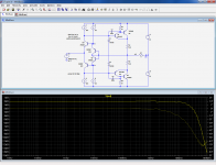
- To ensure a sufficient stability, the compensation capacitors are large enough to hurt the slew-rate, approximately 15V/µs here. Not catastrophic, but not brilliant either.
- Even then, "bits of nastiness" remain visible in the frequency curve: a small accident and ripples that are typical of standing waves going round and round the circuit without proper damping.
- Another problem is the input impedance: although nominally high, in the tens of kiloohm range, it is highly non-linear, and this mandates a very low source impedance, preferably under the ohm, to avoid compromising the good performances.
- Another potential issue is the I/O DC offset: it depends upon the matching of complementary transistors, and could reach tens of mV.
- The diode string had advantages for the initial affectation of the circuit: practically no current is taken below the threshold, but for a normal use, a Vbe multiplier is slightly less inconvenient as it is at least adjustable.
I will begin to examine the solutions in the next post
Attachments
Elvee.
Both circuits look great!
I would say it even can have better figures of THD than my LU Buffer.
This is because the output stage is sziklai, CFB complementary feedback.
I hope people look into this thread.
This is simply a great way to get a good buffer with very low distortion.
Regards, Lineup
Both circuits look great!
I would say it even can have better figures of THD than my LU Buffer.
This is because the output stage is sziklai, CFB complementary feedback.
I hope people look into this thread.
This is simply a great way to get a good buffer with very low distortion.
Regards, Lineup
Member
Joined 2009
Paid Member
Let us first look at the DC offset issue:
it is the easiest to deal with.
To ensure proper compensation, each path between input and output must have homogeneous junctions and they have to operate at similar current densities and have similar dissipations.
This is not difficult to achieve: the positions of Q8 and Q10 have to be swapped, and the diode string (or Vbe multiplier) has to shunt a current of 5mA.
These simple measures will push the offset below 10mV, without any matching and with no temperature dependency.
The other points will require much more fundamental changes.
This renders triples practically compulsory; I do not have much sympathy for this arrangement, but in this case it is practically unavoidable.
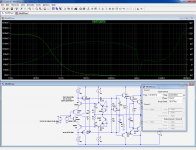
Let us see the result: now, all B-E junctions have their homologous in front of them, in the right order, meaning the compensation is correct, except for one important point: the input transistors are subjected to the full supply voltage, making the compensation ineffective, and stressing the input transistors.
The input impedance has been raised by the Hfe factor, but we still need to properly adress the speed/compensation issue, and we have to solve the voltage/dissipation problem.
We will see in the next post that a clever use of cascoding can satisfactorily resolve these issues
it is the easiest to deal with.
To ensure proper compensation, each path between input and output must have homogeneous junctions and they have to operate at similar current densities and have similar dissipations.
This is not difficult to achieve: the positions of Q8 and Q10 have to be swapped, and the diode string (or Vbe multiplier) has to shunt a current of 5mA.
These simple measures will push the offset below 10mV, without any matching and with no temperature dependency.
The other points will require much more fundamental changes.
- Basically, it involves driving the input transistors with Rush cascodes.
This renders triples practically compulsory; I do not have much sympathy for this arrangement, but in this case it is practically unavoidable.
Let us see the result: now, all B-E junctions have their homologous in front of them, in the right order, meaning the compensation is correct, except for one important point: the input transistors are subjected to the full supply voltage, making the compensation ineffective, and stressing the input transistors.
The input impedance has been raised by the Hfe factor, but we still need to properly adress the speed/compensation issue, and we have to solve the voltage/dissipation problem.
We will see in the next post that a clever use of cascoding can satisfactorily resolve these issues
Attachments
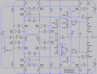
Cascoding is a necessity, it requires two additional transistors but it also brings side benefits:
The transistors of the input "engine" being subjected to small and similar voltage excursions, they are much more linear, and their residual non-linearity is compensated in some measure: this brings a further reduction in THD level.
It is also time to rationalize the compensation, and to further increase the speed.
To do that, we need to establish links between the positive and negative sides of the circuit: this allows one side to help the other when it finds itself unable to generate the transient currents necessary for fast transitions.
This is done by interconnecting the main nodes by capacitors or RC circuits.
The capacitor between the base of the two OP is larger than usual: it is necessary in this case because of the poor complementarity between the 3055 and 2955: it helps equalize the differences between the two polarities, and keeps even order non-linearities down. With better devices, it could have a more normal value.
But even in this case, the THD would remain well under 1ppm for the OP stage alone. By including it in multiple feedback loops together with a similarly clever voltage amplifier, THD levels under the ppb are well within reach.
Perhaps more on that later....
PS:
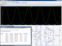
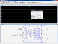
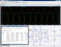
With the mods, the static offset is 87µV (in sim obviously), and the input impedance @1KHz is ~40 Megohm, see last pic:
The transistors of the input "engine" being subjected to small and similar voltage excursions, they are much more linear, and their residual non-linearity is compensated in some measure: this brings a further reduction in THD level.
It is also time to rationalize the compensation, and to further increase the speed.
To do that, we need to establish links between the positive and negative sides of the circuit: this allows one side to help the other when it finds itself unable to generate the transient currents necessary for fast transitions.
This is done by interconnecting the main nodes by capacitors or RC circuits.
The capacitor between the base of the two OP is larger than usual: it is necessary in this case because of the poor complementarity between the 3055 and 2955: it helps equalize the differences between the two polarities, and keeps even order non-linearities down. With better devices, it could have a more normal value.
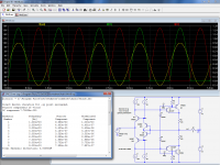
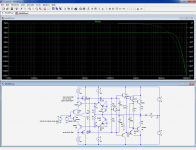
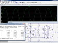
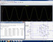
- The first pic shows the result of the improvements on linearity: it is now better than 0.05ppm for 10V output (~40ppb).
- The second pic is the small signal bandwidth: it extends to ~30MHz, but this is rather anecdotal: the important thing is the slew-rate (positive or negative):
- third pic: it now comfortably exceeds 500V/µs, which is about the maximum that can be extracted from a crappy MJ2955/3055 pair without resorting to really exotic techniques or black magic.
But even in this case, the THD would remain well under 1ppm for the OP stage alone. By including it in multiple feedback loops together with a similarly clever voltage amplifier, THD levels under the ppb are well within reach.
Perhaps more on that later....
PS:
With the mods, the static offset is 87µV (in sim obviously), and the input impedance @1KHz is ~40 Megohm, see last pic:
Attachments
Last edited:
It seems to me that one can rearrange the input stage (Q8~Q11) from two Rush cascodes to two LTPs, and get somewhat similar result. It would be like the Class-I without the non-switching bias.
Adv:
1.Simpler circuit, no need for the four bias diodes (Q5/6/12/13)
2.More options of dual transistors of same sexes than mixed sexes (THAT?)
Disadv:
3.Slew rate is limited by current source at LTP's tail.
But if Q8~11 are replaced with complementary JFET pairs, then it is a whole new ball game.
4.If connected as Rush cascodes there are no need of Q5/6/12/13 and I3/5 due to the self biasing nature of JFET.
5.If connected as two LTPs (as John Curl/Sansui diamond differentials), you don't need current sources at LTP tails so slew rate is faster.
6.Disadv: complementary JFETs have few options, low voltage and power rating.
Best Regards,
Edward Tam
Last edited:
Good idea .. with complementary JFET.But if Q8~11 are replaced with complementary JFET pairs, then it is a whole new ball game.
4.If connected as Rush cascodes there are no need of Q5/6/12/13 and I3/5 due to the self biasing nature of JFET.
5.If connected as two LTPs (as John Curl/Sansui diamond differentials), you don't need current sources at LTP tails so slew rate is faster.
6.Disadv: complementary JFETs have few options, low voltage and power rating.
Best Regards,
Edward Tam
This is the way to do it !!!!
For example 2SK170+2SJ74
")
I might setup such a circuit!
I don't think a marginally reduced BOM is really an advantage, and in this circuit only the same polarity pairs need to be matched: P and N devices need not be exact complements (OK, they cannot be totally different but that is not quite the same).1.Simpler circuit, no need for the four bias diodes (Q5/6/12/13)
2.More options of dual transistors of same sexes than mixed sexes (THAT?)
Disadv:
3.Slew rate is limited by current source at LTP's tail.
I think the loss of SR is not a minor issue
It is tempting, but:But if Q8~11 are replaced with complementary JFET pairs, then it is a whole new ball game.
4.If connected as Rush cascodes there are no need of Q5/6/12/13 and I3/5 due to the self biasing nature of JFET.
5.If connected as two LTPs (as John Curl/Sansui diamond differentials), you don't need current sources at LTP tails so slew rate is faster.
6.Disadv: complementary JFETs have few options, low voltage and power rating.
The Vgs matching between N and P devices will be poor, and this means the offset issue will come back.
And with dual complementary FETs, it is not an easy cheapo circuit anymore.
But thanks for your ideas anyway, I am sure they will appeal to some.
I have setup a circuit using 2SK170+2SJ74 for the feedback loop.
I have a small trimpot on the input to adjust DC Offset.
As you say it is very different VGS for the NJFET and the PJFET.
But anyway with IRFP240 + IRFP9240 output the circuit is promising.
It will NOT be as precise as with bipolar transistors
but it will be quite a bit simpler circuit.
I have a small trimpot on the input to adjust DC Offset.
As you say it is very different VGS for the NJFET and the PJFET.
But anyway with IRFP240 + IRFP9240 output the circuit is promising.
It will NOT be as precise as with bipolar transistors
but it will be quite a bit simpler circuit.
I did a version for testing Laterals.I like the first simple circuit....but could it not be made with laterals where you take the signal from the Drains...??
I belive the DC issue could be solved rather simple, by adding a servo that alters the current in on the second pair of current sources
Unffortunately the low VGS made it impossible to fit the diamond inside the loop.
If one wants to use Laterals there should be another solution, like adding BJT drivers to the Gates.
Here is a jFET variant, along with a trick avoiding intersex matching and therefore big offset issues.
The THD is three times worse than the bipolar front-end, but it remains acceptable
Thanks for the effect, but if I am not mistaken the JFETs are all connected as source followers
Here is a Japanese link that shows a JFET Rush cascode front-end driving Toshiba MOSFET. The designer has put in two LEDs to give more voltage headroom to the front-end. One end of the current source is adjustable to take care of the offset. He also "cheated" somewhat with the bias regulator to give some negative feedback. All in all, a designer with many different ideas.
Best Regards,
Edward Tam
In an environment where all nodes move synchronously to within mV of each other, defining a "common" terminal is an interesting exercise in relativity.Thanks for the effect, but if I am not mistaken the JFETs are all connected as source followers
Basically, devices present a transconductance between two ports and two other ports, of which one is common.
But this commonality is completely local, and you are free to define any node as globally common
A good example of what I wanted to avoid.Here is a Japanese link that shows a JFET Rush cascode front-end driving Toshiba MOSFET. The designer has put in two LEDs to give more voltage headroom to the front-end. One end of the current source is adjustable to take care of the offset. He also "cheated" somewhat with the bias regulator to give some negative feedback. All in all, a designer with many different ideas.
What do you think will result if P and N devices do not have exactly the same Vgs at the bias current, and more subtly, what will happen if this Vgs does not track with temperature?
Another interesting question is the overall transconductance of the input compound.
And all of this assumes the jFETS are capable of taking the full voltage swing of the supplies and the resulting dissipation.
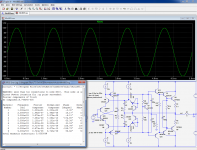
The result is shown:
Even with the perfect complements 2SJ74/2SK170 of the sim, a 6.5mV offset appears (in reality, it would be much worse), and the THD is increased by almost a hundred fold.
Attachments
- Status
- This old topic is closed. If you want to reopen this topic, contact a moderator using the "Report Post" button.
- Home
- Amplifiers
- Solid State
- Alternative buffer topologies