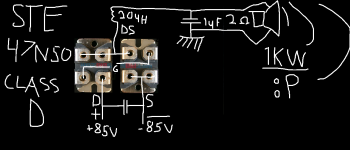
I have today started on a output stage using mosfets that with the right PSU make over 2kW RMS power into a 2 ohm load and over 4kW peak.
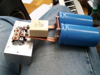
The fets are joined together with busbars made outta flattened copper tubing to minimum stray inductance and maximum current transfer capability.
Now before you say anything, no this is not a serious project, it is all 100% for fun as it will not have any sort of practical use.
Heres a drawing to show how crazy i'm going
Attachments
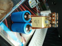
Looks compact.
Current transfer at higher frequencies takes place away from the core of the conductor.
Research "skin effect" and "Litz wire".
Now all you need to do is to build a drive system for the FET's.
Watch for the equivalent gate charge you will need to inject (in the time allowed) to turn them on for good efficiency. This will result in a significant number of peak amps.
Thus begins the interesting tradeoff between peak drive (gate) current, final drive (gate) voltage, switching frequency, supply voltage, and even FET selection (although you have that already)
Have fun learning.
Because:
"The more you learn the less you know"

The basic set up is looking Ok to me.
But the choice of the MosFet is really unpleasant.
It is not just the gate charge, but also the body diodes.
trr =1100ns, Qrr=40uC !!
IMHO a no go for class D.
Don't you observe massive heating, when running at high rails and high signal levels? At 200kHz you might even risk defects.
Ever looked at these?
http://ixapps.ixys.com/DataSheet/DS99349F(IXFN64N50P).pdf
P.S.
No snubbers?
This amp has now been running for several hours on 2x60V rails and have never even gotten warm, its stone cold!
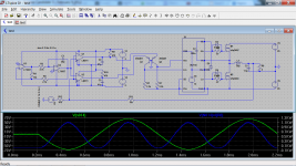
A video: Feedbackless Class D amp with new Power Stage - YouTube
Why the STE47N50 ? well i happened to have 12 of them laying around and as it turns out, the amp is now working ALOT better, its even sounding better.
The feedback loop depicted in the schematic is not actually implemented yet, the amp is running completely open loop.
Using devices you have on hand is always worth a trial.
The concerned/critical load area would start at output currents higher than the filter ripple.
Seeing +/-60V, 20uH, 200kHz, means a filter ripple of +/-3.75A.
Most likely the shown load situation of your video does not have much content above that.
For 2kW into 2 Ohms you would need to run around +/-90V rails and drive it close to clipping into the two Ohms.
Well, for first I would propose to stay with +/-60V, but change the load.
For unscientific testing you can put a 2 Ohms resistor to the output and in parallel a resistive divider which feeds your speakers in attenuated mode while running the amp up to clipping area.
This allows to operate the amp at high power and listen to it without blowing your ears and/or speakers, walls, neighbors....
For detailed examination of the hard switching events and device SOA, I am usually forcing the amp to deliver DC output currents up to max output current.
I am using DC loads, because this allows examination in steady state without modulation. Unfortunately that's tougher than music program.
Most realistic is Eva's approach to examine the modulated switching events, but the resulting pictures are more difficult for correct interpretation.
I tend to use a dummyload and a 1Hz sine to see what the PWM gen is doing, but i suppose a pot wired between the two 5V rails would work too.
I ac tually have no clue what inductance the coil i use it, its a dc bus filter choke from a 3.5kW 48V 73A smps, around 5cm diam and is light green with a yellow rim.
The amp does work better with a T106-2 core though.
I ac tually have no clue what inductance the coil i use it, its a dc bus filter choke from a 3.5kW 48V 73A smps, around 5cm diam and is light green with a yellow rim.
The amp does work better with a T106-2 core though.
Last edited:
I tend to use a dummyload and a 1Hz sine to see what the PWM gen is doing
...basically also an option for examining the switching details.
but i suppose a pot wired between the two 5V rails would work too.
yupp, but in both cases (1Hz or DC ) you have to take care for supply rail pumping !
I tend to put my load for DC examination not to ground but to the upper rail and have the pot adjusted to make the amp generating a DC output voltage close to the rail.
By this you force a DC current load (Idc=(Urail-Uout)/R) which will run currents through the body diode of the upper Mosfet during dead time. Examination of Ugs and Uds of the lower switch allows to see all trouble of the switching stage during hard switching.... and there is always imperfection..
But that's tough load for the lower switch, because you force the worst load situation not just for some ms like music program , but continuously. At high currents such load is allowable only for short time.
In case of short comings in gate drive and/or layout/snubbering it may cause defects almost immediately.
My current power stage with IRFB4115 is running at 400kHz and allows this with +/-60V rails and 30A DC for few seconds only.
Easily long enough to catch it with the analog screen memory of the old fashioned scope that I use, but you cannot let it run in a careless manner.

Hi Pafi,
I am not convinced that this method to overcome the body diode issues is applicable here.
The N-Chanel does not shunt the body diode during dead time.
A precise adjustment of effective zero dead time (or even slight shoot through) appears difficult to me when driving such heavy MosFets with the IR21xxx.
...but of course worth a trial...
The N-Chanel does not shunt the body diode during dead time.
Yes, but it can be a short time, and the stored charge can't fully build up, the following reverse recovery must be much faster then the specified. Reverse recovery charge can't be higher than the stored charge, and stored charge is less then current during dead time*dead time (assuming full shunting effect during conduction).
This is not a solution, just masks the problem at light load.
- Status
- This old topic is closed. If you want to reopen this topic, contact a moderator using the "Report Post" button.
- Home
- Amplifiers
- Class D
- Tekko goes crazy