Ive been reading this forum and have greatly enjoyed all the experience of the members here.
Here is my 2nd attempt this time I really want to learn.
Criteria is a 100W amp into 8Ohm, with acceptable performance,
I dont expect a great result as this is a first and very new to me.
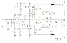
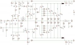
I wanted to keep it simple. I drew have 2 circuits,
Ive made a toner transfer pcb of the first circuit and will build it as
time allows.
The second circuit is just a thought, to be more flexible at various supply voltages.
Ive only spent about 2hrs on second circuit.
Pls inform of changes I should make.
Ive tried to do the best I can, but I need advice.
Here is my 2nd attempt this time I really want to learn.
Criteria is a 100W amp into 8Ohm, with acceptable performance,
I dont expect a great result as this is a first and very new to me.
I wanted to keep it simple. I drew have 2 circuits,
Ive made a toner transfer pcb of the first circuit and will build it as
time allows.
The second circuit is just a thought, to be more flexible at various supply voltages.
Ive only spent about 2hrs on second circuit.
Pls inform of changes I should make.
Ive tried to do the best I can, but I need advice.
Attachments
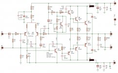
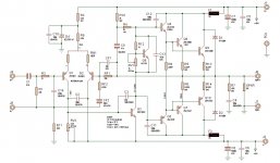
Bias pot looks correct and can be replaced with a fixed resistor once the value is established. A few things... The CCS for the IPS might be a bit low, the input transistors would like at least 1mA each. Ft drops off if collector current is too low, take a peek at Ft or GBW compared to Ic in a datasheet. Placing a pot in series with R2 will adjust the DC output offset by adjusting the IPS bias current, allowing the mirror to balance the difference and still keep equal degeneration in the IPS. Ex. If the DC output is +1V, Ve of Q2 is 1.6V and Ve of Q1 is 0.6V so Q1 tries to conduct more than Q2. Increasing the IPS CCS current allows more base current to Q3, making the output track further negative, turning on more Q2 and establishing a balance where the proper amount of base current is allowed to flow to Q3 so as to create 0Vdc output. Also Q3 needs an emitter resistor, ~=R4. R9 could be larger, ~2mA or so. When the output is driven completely to the +rail as in clipping, Q12 will saturate. Adding a base resistor ~1K to Q12 will prevent this saturating situation from effecting the IPS CCS. Miller Cdom, C3 seems to be a bit large. Also a cap, ~47 - 100uf, across R8 will help prevent cross-conduction of the output transistors at high frequency testing. Some local decoupling right at the output transistors wouldn't be a waste either.
Last edited:
Ive been reading this forum and have greatly enjoyed all the experience of the members here.
Here is my 2nd attempt this time I really want to learn.
Criteria is a 100W amp into 8Ohm, with acceptable performance,
I dont expect a great result as this is a first and very new to me.
I wanted to keep it simple. I drew have 2 circuits,
Ive made a toner transfer pcb of the first circuit and will build it as
time allows.
The second circuit is just a thought, to be more flexible at various supply voltages.
Ive only spent about 2hrs on second circuit.
Pls inform of changes I should make.
Ive tried to do the best I can, but I need advice.
You are sensible to use conventional designs for a first amp.
First, if you don't have the books by Douglas Self and Bob Cordell then buy them!
My comments on the first circuit.
R3 could be much lower resistance to reduce noise. 1K at most, preferably less.
RF1 and RF2 similarly could be lower. Cost is extra power dissipation so need to ensure adequate power capability.
No output inductor?
C1 and CF2 are electrolytic capacitors. Read Self on this for a reasonable presentation of when capacitors matter and when it is "fetishism".
Second circuit similar except R15 and R10 could be increased to reduce noise.
Samuel Groner has an excellent website with a must-read paper on this topic.
BTW. What did you use to do the circuit boards?
Best wishes
David
Last edited:
Again thanks to all that have posted here, Im trying to implement most of the improvements suggested.
Thanks for the advice on the Audio Amplifier Books, Ill be buying at least one.
They are pricey here and Ill invest in another as finaces allow.
As for the Miller cap of 100pf, I must admit that Ive either not learned to calculate it in my studies, or just forgotten how.
So I just used the arbitrary 100pf.
If the value can be calculated easily Id love to know how.
If its to complex , Ill trial and error it, when the amp is built.
Any more info here would be great.
I use Proteus (Isis and Ares), I mainly work with digital circuits, and Proteus helps me cut down development time, simulating microcontrollers.
lol, Ive never been lucky enough to write a program for one med/large microcontroller project that didnt need its fair share of fault finding.
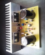
Ive etched my pcb of circuit 1 and will be drilling and soldering it during the week, It wont be great, but Im still excited to build it.
Ill supply it with my newly made DIY Bench Supply for initial testing.
hehe I think the Supply cost me more to build than if I bought one.
Ill only etch circuit 2 after a good couple of revisions.
Thanks for all your help.
First, if you don't have the books by Douglas Self and Bob Cordell then buy them!
Thanks for the advice on the Audio Amplifier Books, Ill be buying at least one.
They are pricey here and Ill invest in another as finaces allow.
Miller Cdom, C3 seems to be a bit large.
As for the Miller cap of 100pf, I must admit that Ive either not learned to calculate it in my studies, or just forgotten how.
So I just used the arbitrary 100pf.
If the value can be calculated easily Id love to know how.
If its to complex
, Ill trial and error it, when the amp is built.Thanks, what typical size resistor would you advice, Im not sure how much voltage to develop over the current mirror.Also Q3 needs an emitter resistor
Any more info here would be great.
BTW. What did you use to do the circuit boards?
I use Proteus (Isis and Ares), I mainly work with digital circuits, and Proteus helps me cut down development time, simulating microcontrollers.
lol, Ive never been lucky enough to write a program for one med/large microcontroller project that didnt need its fair share of fault finding.
Ive etched my pcb of circuit 1 and will be drilling and soldering it during the week, It wont be great, but Im still excited to build it.
Ill supply it with my newly made DIY Bench Supply for initial testing.
hehe I think the Supply cost me more to build than if I bought one.
Ill only etch circuit 2 after a good couple of revisions.
Thanks for all your help.
Nearly done with Circuit One.
I have no Data on the heatsink I'm using.
So I'll Take Heat readings and work backwards to get its thermal resistance,
so I'll know for future, my supplier sells them for a reasonable price.
Circuit One is just a test circuit, I'm not intending to use It for Home.
Just A Project to help me understand some aspects.
Once I'm happy with Circuit 2, I'll be interested to compare it to Circuit 1.
Its been great fun, but I'll not have time to test it till monday.
Ill first supply with 30V-0-30V DC from my Lab Supply with Ilimiter set low.
then fault find if nessesary
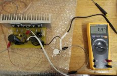
I powered up Circuit 1 on 30V-0-30V bench supply and so far, its ok.
I played some music on it and it played.
Im aware that this amp isnt high quality but its been fun and would like to take some measurements.
But how do I measure output noise,
I got access to multimeters and scope, no fft function.
I tossed a AC Voltmeter and got 1.4mVrms , 10min later when I looked again it was 0.9mVrms , this is with input pot set to min.
Crappy pot tho, doesnt seem to goto 0R.
Ill connect it to bridge and 30V-0-30V AC transformer.
thanks
Attachments
In the spirit of fun and diy,
I continue to play with this circuit.
Some changes have been made.
Is 60mWq ok for 2n5401's
lol ignore random component numbers, product of changing my mind.
Q1,2 Running at ~ 60mWq (Ic ~= 1mA)
Q11 Running at ~ 60mWq (Ic ~= 2mA) (Vce = (60 -(2mA x 15000)))
Q13,14 Running at ~ mWq neglectable
Q3,12 Running at ~600mWq (10mA x 60)
Q15,16 Running at ~330mWq (Ie ~= (0.6 x 2) / 220) = (5.4mA)
Q4,5 Running at ~500mWq (Ie ~= 6.5mA + (0.5mA x 4) per Base) = (8.5mA)
Q19,20 `\
Q6,7 ````\ Running at ~ 2.4Wq (Ic ~= 40mA per Transistor)
Q9,10 ```/
Q17,18 `/
Pls advice is Currents at Transistors are ok for opperation,
and if power diss, is ok. (0.6Wq at Vas transistor worries me abit)
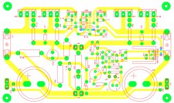
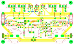
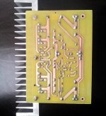
I struggle with PCB layouts, but I keep trying.
This needs revision, but Ill share anyway, maybe theres some comments,
Like moving tracks, components,
I'm hoping that its heading in the right direction, for a beginner.
This project has been so much fun, and ofc I have some excitement
and hope that the result is reasonable, but even if it isnt,
I still enjoy it.
I continue to play with this circuit.
Some changes have been made.
Is 60mWq ok for 2n5401's
lol ignore random component numbers, product of changing my mind.
Q1,2 Running at ~ 60mWq (Ic ~= 1mA)
Q11 Running at ~ 60mWq (Ic ~= 2mA) (Vce = (60 -(2mA x 15000)))
Q13,14 Running at ~ mWq neglectable
Q3,12 Running at ~600mWq (10mA x 60)
Q15,16 Running at ~330mWq (Ie ~= (0.6 x 2) / 220) = (5.4mA)
Q4,5 Running at ~500mWq (Ie ~= 6.5mA + (0.5mA x 4) per Base) = (8.5mA)
Q19,20 `\
Q6,7 ````\ Running at ~ 2.4Wq (Ic ~= 40mA per Transistor)
Q9,10 ```/
Q17,18 `/
Pls advice is Currents at Transistors are ok for opperation,
and if power diss, is ok. (0.6Wq at Vas transistor worries me abit)
I struggle with PCB layouts, but I keep trying.
This needs revision, but Ill share anyway, maybe theres some comments,
Like moving tracks, components,
I'm hoping that its heading in the right direction, for a beginner.
This project has been so much fun, and ofc I have some excitement
and hope that the result is reasonable, but even if it isnt,
I still enjoy it.
Attachments
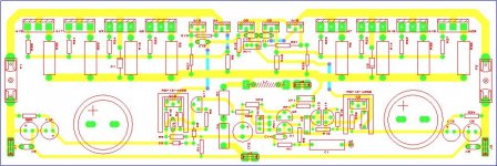
The only way to learn how to do PCB layout, is to do PCB layout Trial and error. You are doing well so far.
Your power dissipation sounds OK to me. As long as your VAS transistors have a little heatsink, as they do in your layout, they will be fine. A good rule of thumb is can you hold your finger on the transistor when its operating? If you can't, it's too hot.
Trial and error. You are doing well so far.Your power dissipation sounds OK to me. As long as your VAS transistors have a little heatsink, as they do in your layout, they will be fine. A good rule of thumb is can you hold your finger on the transistor when its operating? If you can't, it's too hot.
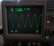
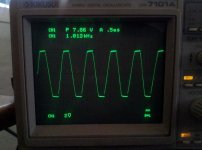
Circuit 1 progress,
I finally got some time to put circuit 1 on a scope.
Supply was 30V-0-30V Unregulated with 6800uF smoothing.
Input was 1kHz sine wave from signal generator.
Output was 8R 100Watt Resistor in sml heatsink box.
Scope on x10 Probe.
Vas used was 2SC3953E ft=400Hmz, Vce(max)=120V, Cob= 2.1pf, hfe=100-200
http://www.composants-electroniques.com/docs/pdf/10281956.pdf
At first used 6800uF smoothing caps on supply.
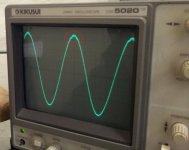
I got ringing as posted in attachment with output higher than ~30Vpk.
I then added my loose unreg supply board, with extra ~20mF smoothing.
The ringing was still there, so I guess its not due to supply ripple.
After staring at circuit for too long I decided to change input transistors and Vas transistor.
Ringing was still there with other input transistors,
so I change 2SC3953 Vas to a MJE340.
With MJE340 Vas ringing was gone.
Output could reach 77Vp-p (93W into Resistive load) before clipping.
Gain is even from 20hz to past 20kHz.
I finally got some time to put circuit 1 on a scope.
Supply was 30V-0-30V Unregulated with 6800uF smoothing.
Input was 1kHz sine wave from signal generator.
Output was 8R 100Watt Resistor in sml heatsink box.
Scope on x10 Probe.
Vas used was 2SC3953E ft=400Hmz, Vce(max)=120V, Cob= 2.1pf, hfe=100-200
http://www.composants-electroniques.com/docs/pdf/10281956.pdf
At first used 6800uF smoothing caps on supply.
I got ringing as posted in attachment with output higher than ~30Vpk.
I then added my loose unreg supply board, with extra ~20mF smoothing.
The ringing was still there, so I guess its not due to supply ripple.
After staring at circuit for too long I decided to change input transistors and Vas transistor.
Ringing was still there with other input transistors,
so I change 2SC3953 Vas to a MJE340.
With MJE340 Vas ringing was gone.
Output could reach 77Vp-p (93W into Resistive load) before clipping.
Gain is even from 20hz to past 20kHz.
Attachments
Last edited:
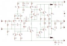
Im changing the values of:
R3
Cf2
C14
Q3 will be getting 22R Emitter resistor.
Q3 was changed to MJE340.
R7 was changed from wirewound to carbon.
R8 was changed to 150R 1W carbon.
I want to change cf2, not polarised electrolytic, Any ideas?
Must D4 be grounded to supply grnd or signal grnd, I didnt see a reason to connect to signal grnd,
but still wonder.
Regards
Last edited:
Ringing goes when changing from 2.1pF for Q3 to unspecified Cob for Q3.
I'll bet the increased Cob effectively added Cdom and increased the stability margins by reducing the open loop gain at high frequencies.
Instead go back to your low Cob for Q3 and increase Cdom across BC junction. Try 47pF to 100pF.
I'll bet the increased Cob effectively added Cdom and increased the stability margins by reducing the open loop gain at high frequencies.
Instead go back to your low Cob for Q3 and increase Cdom across BC junction. Try 47pF to 100pF.
I replaced C3953,
I then replaced Cdom with 47nf then 68nf then 100nf,
the top of the waveform rounded more but still rang at closer to max output.
Maybe im missing something or maybe I have bad copies of the transistors.
I put back the MJE340 and 22pf silver mica and no ringing at all, even to past clipping.
For now I think Ill be satisfied as it is.
When I buy in other low cob transistors, Ill revisit this.
Also changed C9 to 100uf, Cf2 to 470uF
I reset Bias and dc offset to 75mA measured with ammeters instead of fuses.
Before changes, the amp made a corcerning thump at switch on, and switch off.
After changes and settings noted here and previous posts, the thump is very low.
Im happy,
Next is to build circuit two, which is evolution of circuit 1, but still very conventional.
Ill see if all the improvements in circuit 2 makes a big enough improvement to be noticeable.
Regards
I then replaced Cdom with 47nf then 68nf then 100nf,
the top of the waveform rounded more but still rang at closer to max output.
Maybe im missing something or maybe I have bad copies of the transistors.
I put back the MJE340 and 22pf silver mica and no ringing at all, even to past clipping.
For now I think Ill be satisfied as it is.
When I buy in other low cob transistors, Ill revisit this.
Also changed C9 to 100uf, Cf2 to 470uF
I reset Bias and dc offset to 75mA measured with ammeters instead of fuses.
Before changes, the amp made a corcerning thump at switch on, and switch off.
After changes and settings noted here and previous posts, the thump is very low.
Im happy
,Next is to build circuit two, which is evolution of circuit 1, but still very conventional.
Ill see if all the improvements in circuit 2 makes a big enough improvement to be noticeable.
Regards
Attachments
- Status
- This old topic is closed. If you want to reopen this topic, contact a moderator using the "Report Post" button.
- Home
- Amplifiers
- Solid State
- Second attempt at Building my own amp from scratch