Please review this design where my main concerns are.
Thermal stability.
Cheap easy to source parts.
Three files attached:
The amp.
Doc about the amp.
A bridged version.
Thermal stability.
Cheap easy to source parts.
Three files attached:
The amp.
Doc about the amp.
A bridged version.
Attachments
I think you made a good summarizing job yourself.
With such small emitter degeneration resistors (I understand why they are necessary for good performance), the design will be quite sensitive to initial mismatches and thermal tracking issues.
Regarding electrical stabilty, I think it would be wise to tie C1 to the output of U1.
Closing the complete loop in HF would probably stress U1's stabilty margins to the limits.
Thanks for your inputs.
Resistor degenerative values. I don't really know what is a right value for a good compromise, more stability / less max output power. Any idea ?
About C1.
My first design had no C1 capacitor. I added it for band limiting, it gives some better THD at 20KHz, about none at 1KHz.
I did not thought about tying C1 at the output of U1. I just tried this, it lowers THD 1KHz to 0.002% ( from 0.00016% when tied at the overall output ). I do not understand the reason why..
what are the goals of the design:
load Z range, frequency response, Power, acceptable distortion limits...
is Class B bias a design requirement?
Thermal stability..
50 KHz.
Low power ( tri amplification ).
Class B for efficiency and fun to study its thermal stability issue ( a topic mostly overlooked or handwaved ).
Class B efficiency means reasonable heatsinks and PSU costs which is a large part of amplifier systems cost.
Member
Joined 2009
Paid Member
Looks nice. If I were to offer some suggestions for changes to try out:
a) increase emitter degeneration from 0.01 (which is probably the resistance of the wiring) to 0.22
b) you need some parasitic compensation caps to stop the CFP oscillation - a 47pF cap between base and collector for Q1 and for Q2.
c) you can increase the voltage swing at the output with the addition of some resistors. You have CFP output where the voltage gain from Q1 (and Q2) is 100% applied to local feedback from the collector of Q5 (Q6) to the emitter of Q1 (Q2). So break this link with a resistor and tie the emitter of Q1 (and Q2) to the output via another resistor each. With the right choice of values you can release a little of the voltage gain from the CFPs to increase output swing - x2 would probably be a good amount.
Since you have gobs of fdk from the op-amp to keep distortion down the above changes likely won't be an issue to the sonics.
d) add an input rf filter and a zobel to the output
e) the current sources will be more stable with a small capacitor between bse of Q7 (Q10) and base of Q8 (Q9) of value around 1nF
f) maybe PSRR of the amp can be improved by adding some bigger caps to the current sources in the right places
g) make one current source adjustable, e.g. R2, so that you can set dc-offset. Or you could turn one of the current sources into a dc-servo if you want to get fancy by adding another transistor or two.
Thanks, Bigun for your many inputs, I agree with.
About a x2 CFP current booster. I had a go at this.
From LTspice, I saw, one needs very smal resistor values in order to NOT lower much the THD ( small resistor values below 50 ohms ).
And using 2 resistors ( instead of 4 as I saw in many designs ) is much better.
This x2 CFP has bad reputation about thermal stability ( Rod Elliot says it is a no no ).
I don't know yet how to study this.
Member
Joined 2009
Paid Member
This x2 CFP has bad reputation about thermal stability ( Rod Elliot says it is a no no ).
I don't know yet how to study this.
Sometimes you have to try things that conventional wisdom says is bad - otherwise you just get the same old same old.
I don't know what the issues are myself either. But thermal stability is something you can simulate. Right click on the name of the device, e.g. "BD139" and then in the edit box change it to "BD139 temp=40" to set the temperature of the device for the simulation.
You may need temperature compensation, i.e. the bias diodes have to go on the heatsink with the output devices.
Spice is very limited about temperature simulation.
Indeed one can set a temp at each BJT junction. However this temp will not change during a simulation showing how things go when BJT's get hot or cool down.
The bad joke is Spice considers temp as a variable. Temp is actually a constant.
The only thing one can do more in a Spice simulation, is implementing the Vbe decrease with junction temperature, adding device temperature models.
Spice is only giving some help asking for many simulations and manual side work.
Bigun provided you with very useful and sensible guidelines.Thanks, Bigun for your many inputs, I agree with.
About a x2 CFP current booster. I had a go at this.
From LTspice, I saw, one needs very smal resistor values in order to NOT lower much the THD ( small resistor values below 50 ohms ).
And using 2 resistors ( instead of 4 as I saw in many designs ) is much better.
This x2 CFP has bad reputation about thermal stability ( Rod Elliot says it is a no no ).
I don't know yet how to study this.
But in a way, he goes against his own advices:
Sometimes you have to try things that conventional wisdom says is bad - otherwise you just get the same old same old
Increasing the degeneration resistors will also increase the distortion: optimum distortion is attained with zero resistors, and minimal quiescent current -as close to pure class B as real devices allow-
Adding gain to the CFP will also introduce degeneration resistances, unless ridiculous amounts of power are spent in the resistive dividers.
The dividers will also reduce further the already small amount of feedback from the degeneration resistors.
All that amounts to dumbing down of the original scheme.
The clever thing to do is to include those advices without dumbing down the initial quality: creating voltage gain in the output stage without degrading the linearity or decreasing the thermal feedback from the emitter resistors.
Active feedback blocks might be an answer, that attenuate the main signal by the required gain, but amplify the difference across the degeneration resistors.
M J Renardson has some nice ideas about those subjects.
:
Increasing the degeneration resistors will also increase the distortion: optimum distortion is attained with zero resistors, and minimal quiescent current -as close to pure class B as real devices allow-
This is not soo bad.
Near zero resistances give 0.00016% THD while 0.22 Ohm resistances give 0.00020%
:
Adding gain to the CFP will also introduce degeneration resistances, unless ridiculous amounts of power are spent in the resistive dividers.
Adding a x2 gain is indeed a THD killer and a power grabber.
I'll look at the active block feeback.
Is the idea,. Using large resistor values for the divider with a voltage follower giving the divider voltage under a low impedance ?
Member
Joined 2009
Paid Member
Near zero resistances give 0.00016% THD while 0.22 Ohm resistances give 0.00020%
Both of these THD numbers are so small as to be nearly meaningless - in my opinion. The placement of wires in the chasis are worth more THD than this.
It's quite fun playing in spice and watching those harmonics disappear into the noise but it can be a Red Herring.
There will be many different opinions, but I think THD of 0.03% is good enough if it's mostly 2nd and 3rd harmonic.
Indeed very low THD is a myth.
I tried a x2 using a resistor divider 20 Ohm 20 Ohm that grabs 5% of the output power from the 2 Ohm load.
This gives a 0.004% THD.
I tried a x2 with an active block. This gives no compromise about THD and output power.
Hower this active block was implemented with a Spice voltage source.
To make a real block will not be as easy as an Op amp because it should provide more than +-100mA for the driver transistors emitters.
If you use a CFP with gain, realistically, the gain should be kept very small, in order to keep things thermally stable. The gain arrangement with an external divider increases it with respect to the power transistors as current from the power transistors seen by the driver emitter resistor reduces by the same amount as the gain introduced into the circuit.
In modern power transistors employing a LAPT or ring emitter construction, the equivalent emitter bulk resistance is actually larger than with common power transistors - these fast 2nd breakdown resistant devices are constructed as arrays of smaller transistors with built-in emitter resistors. They often amount to 0.1-0.15 ohms, depending on device size, so on the same order of magnitude as external emitter resistors. This makes the tempco of these power transitors somewhat lower than usual, alowing for a small gain addition, without loss of thermal stability, but the numbers are typically around 1.1-1.2 or so. Often this is enough to cover the rail loss of the previous stages. The added advantage of this small gain is that minimal degeneration to the driver transistors and power loss are introduced.
It should be noted that the choice of 'driver' transistors can be important as they also have bulk emitter resistance that may not be trivial in amount, and it also plays a role in thermal stability. The more exotic very fast drivers can sometimes be problematic in this regard when employed in a CFP with gain structure. Any degeneration solely to the driver transistors reduces the gain of the drivers, but this also means they are less sensitive to the feedback caused by the power transistor collector current passing through the remaining portion of the emitter current. Thermal stability of the current through the drivers increases, but the thermal stability of the current through the power transistors decreases - as they are more loosely coupled electrically.
Last edited:
I've been playing with op-based amplifiers a bit. My first attempt was simply an NE5534 with integrated darlingtons at the output (TIP147/149 I think). This turned into a complete failure because, after taking care of oscillations, the darlingtons were impossible to thermally stabilize. A darlington has 2xVBE from input to output thus twice the sensitivity to thermal changes, plus the integrated device has driver and power transistor thermally coupled which now seems like a very stupid idea to me. After the PCB burst into flames after playing for a while (it was powered from a 400VA toroid transformer) I abandoned the project.
I now have mchambin's circuit on the breadboard and did some THD measurements.
Some changes to the original schematic:
-the CFP oscillated badly so I added comp caps to the drivers; the BD136 (negative side) I found needs something around 400pF for lowest THD while the BD139 is happy with just a few tens of pF
-LME49860 and OPA552 were used as op-amp
-power supply is limited to +/-13V (maximum output from my stabilized lab power supply)
-stopper resistors were added (100R to the op-amp's output and 10R to each driver base)
Attached are the THD results with comparison to loopback connection on my Xonar DX soundcard. The test was conducted both with open output and 8R dummy load; interestingly this only caused minimal change to the THD. Distortion becomes much smaller at higher frequencies; I don't know if this is due to the 100uF output capacitor or just a quirk of the measurement software (Visual Analyzer + WaveSpectra).
I also compared non-inverting and inverting topology; now noticable changes in THD were observed. Also the LME49860 was compared to a OPA552; the latter had about the same THD. I conclude that the major source of distortion must be the output stage and there is a limit as to what extent the op-amp's feedback can deal with it.
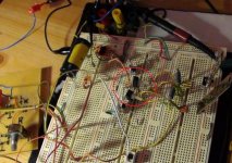
The bias voltage is non-adjustible as in mchambin's original design. As you can see on the picture the drivers and diode-connected bias transistors are thermally coupled. The circuit seems to be very stable now.
A few ideas I want to try out:
-insert VBE multiplier and find out optimal bias voltage
-use error-correction output stage
Any further ideas/comments on how to improve this circuit?
I now have mchambin's circuit on the breadboard and did some THD measurements.
Some changes to the original schematic:
-the CFP oscillated badly so I added comp caps to the drivers; the BD136 (negative side) I found needs something around 400pF for lowest THD while the BD139 is happy with just a few tens of pF
-LME49860 and OPA552 were used as op-amp
-power supply is limited to +/-13V (maximum output from my stabilized lab power supply)
-stopper resistors were added (100R to the op-amp's output and 10R to each driver base)
Attached are the THD results with comparison to loopback connection on my Xonar DX soundcard. The test was conducted both with open output and 8R dummy load; interestingly this only caused minimal change to the THD. Distortion becomes much smaller at higher frequencies; I don't know if this is due to the 100uF output capacitor or just a quirk of the measurement software (Visual Analyzer + WaveSpectra).
I also compared non-inverting and inverting topology; now noticable changes in THD were observed. Also the LME49860 was compared to a OPA552; the latter had about the same THD. I conclude that the major source of distortion must be the output stage and there is a limit as to what extent the op-amp's feedback can deal with it.
The bias voltage is non-adjustible as in mchambin's original design. As you can see on the picture the drivers and diode-connected bias transistors are thermally coupled. The circuit seems to be very stable now.
A few ideas I want to try out:
-insert VBE multiplier and find out optimal bias voltage
-use error-correction output stage
Any further ideas/comments on how to improve this circuit?
Attachments

- Status
- This old topic is closed. If you want to reopen this topic, contact a moderator using the "Report Post" button.
- Home
- Amplifiers
- Solid State
- Another op amp based amplifier.