Hi guys,
I'm more of a valve guitar amplifier building kind of guy, although I'm more technical than a musician, however I'm working on my first PCB build and I know PCBs are a lot more popular with audiophiles than guitar amp builders. I was hoping to get some advice from the community here about how best to route my heaters on my PCB so as to best avoid coupling hum into the other components.
I have 5 preamp valves to go into a PCB, at 12V ac, 150mA each, 750mA total. I know that's quite a lot compared to many HiFi amps, meaning I can't run them all on DC, the high current means stronger magnetic fields, and the gain is higher than in HiFi, so the situation is far from ideal.
So far, what I've considered is having the 2 tracks running parallel to each other either side of the PCB to keep them close (the drawback being that they would obstruct both sides of the board, so I couldn't run any signal wire across it) or having them next to each other on the same side of the PCB; and surrounding the whole thing with a ground trace to shield the rest of the PCB, grounded separately to the signal (the drawback of this being that it takes lots of space on an already tight PCB); or just wiring them up with a twisted pair of wires held away from the PCB somehow and coming vertically down to the valve sockets.
How do you guys normally do this, or do you just get away with a simple solution because of your generally smaller currents and lower gain?
Cheers,
Matt
You should be able to drive it with a simple regulator. If you do, remember that you have to drop the current rating of the transformer by .707, so you need a transformer with at least 1.4 times the current draw of the heaters. In this case you need a transformer with a rating greater than 1.06A, so figure 1.5A or better.
If you can find a 1.5A 10V transformer, you could get 1.414*10-VkaX2 or if you use Schotkey diodes 14.14-2*.3=13.54V.
You can get by with a regulator that has 1V dropout (12.54V-losses) if you use sufficient bulk storage capacitors, but you will have high charging currents that tend to produce more noise, so you are better off using an LDO and relaxing the bulk storage requirement and longer charge duty cycle, or going with a higher voltage rated transformer.
A 12.6V transformer will give you 17.8V, and you won't need low drop diodes, so figure 16.5V peak after rectification. If you adjust your capacitor value to control ripple (I had to look up- the formuale Vrpp = I / (2f * C)) you can set the minimum voltage at a half volt or so above the minimum for proper regulation and limit power dissipation.
If your regulator (eg 7812) drops out at 2.0V and has a tolerance of 4%, you need to account for 2+.48V drop across the regulator. So figure your minimum voltage accounting for ripple needs to be 3V above output, or 15.6V so you can have 2.2V ripple. This would require 2841uF (60hz line) according to the formulae Vpp=C * I / t
In addition if you use a 7812 it will not put out 12.6V, however you can place a standard rectifier in the ground connection and add a reistor from the output to the diode to swamp the ground current from the regulator. Figure 10mA of current through thte resistor to swamp the 1mA operating currentof the 7812, so you need a 100R resistor from output to the anode of the diode/ground of the regulator.
Power dissipation becomes 3*0.75= 2.23W so a small heat sink will suffice.
Last edited:
I would use twisted wire, and make sure it doesn't run parallel to any PCB signal traces for any appreciable distance. Roughly, the spacing from the PCB should be no smaller than the twist length.
 Highly recommended and the way I always do it..
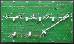
So far, what I've considered is having the 2 tracks running parallel to each other either side of the PCB to keep them close (the drawback being that they would obstruct both sides of the board, so I couldn't run any signal wire across it)
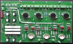
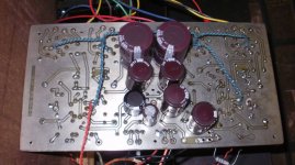
The way to go is to make pairs of holes in the PCB very close to each tube socket. Then use jumpers made of twisted pairs of solid wires to jumper the AC current. You'd raise the twisted pair off the plane of the PCB as far as you can. At least 1/2 inch.
I don't think any PCB layout can out perform jumper wires unless you go "exotic" with six layer PCB designs and interleave the heater traces so they are stacked. Stacked traces can be even closer together than twisted wires.
What matters is (1) the core to core separation, for a twisted pair that is twice the insulation thickness and (2) the distance between the pair and the signal trace.
Last edited:
If you can find a 1.5A 10V transformer, you could get 1.414*10-VkaX2 or if you use Schotkey diodes 14.14-2*.3=13.54V.
Actually, this assumes a zero conduction angle. I.e. the diodes conduct an infinite amount of current for an infinitesimal amount of time. That's not the case in real life. Typically, you end up with 1.2~1.3x Vrms rather than the theoretical sqrt(2)*Vrms on the reservoir cap.
In addition, mains variations will cause the 10 V to drop to more like 9~9.5 V under worst case conditions. Allowing for 2 V ripple, 2.5 V dropout, 12.6 V out, 10 % mains variation, 1.4 V diode drop (full-wave rectifier), you'll end up needing a 17.2 V transformer. Go with an 18 V...
Of course, the worst case for power dissipation in the regulator is the case where the mains are 10 % high. So (18*1.1*1.3-(1.4+12.6))*0.75 = 8.8 W. This assumes the transformer puts out 18 V when loaded. If it's slightly higher, the power dissipation will be slightly higher as well.
As far as PCB layout goes: Keep the heater traces fairly wide (40 mil or so) and as close together as reasonably possible (10~12 mil spacing) on the same layer. This minimizes the loop area formed by the heater traces (the loop being the loop the heater current follows). Minimizing the loop area minimizes the inductance of the loop, hence, minimizes any inductive coupling between the heater loop and everything else.
Same goes for the signals. Route signal forward and return as close together as possible. Again to minimize the loop area, hence, inductance. The mutual inductance between the heater loop and signal loop will cause coupling between the two. That's why it's important to minimize the inductance.
Beware that you'll need a fair amount of spacing between traces carrying high voltage. It's the potential difference between the traces that drives the spacing, not the absolute value of the voltage. So you can route, say 220 V and 250 V close together (the difference is only 30 V) but 220 V and ground will have to be separated further. This is the best site I've found on the matter: PCB Trace Spacing for High Voltage. Note that if you make your own board, you'll either have to allow for more spacing or apply a conformal coating to the board after you're done. If you have the board fabricated elsewhere, make sure to get a soldermask on it as it'll act as a conformal coating.
~Tom
- Status
- This old topic is closed. If you want to reopen this topic, contact a moderator using the "Report Post" button.
- Home
- Amplifiers
- Tubes / Valves
- Any tips for routing heaters on a PCB