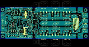
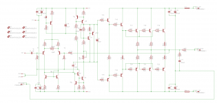
Made a layout for an EF amplifier with 60-100 W output into 8 ohm.
Most is based on Bob Cordells excellent examples in his book but with a few changes and additions here and there, some ideas are from this very forum, see Vbe multiplier. So nothing original and nothing I myself can take credit for.
However, interested in some (positive)critique of my layout.
It is not perfect but should be halfway decent, I hope so anyway.
Attachments
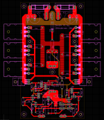
Why the big gap between the + & - power rails?
You repeat the same "gap" in the voltage amp stage.
Both these aerials will inject interference into all the adjacent circuits.
The very wide spacing of the outputs devices demands an enormously wide/tall heatsink.
Move the L//R of the Thiele Network off board.
You repeat the same "gap" in the voltage amp stage.
Both these aerials will inject interference into all the adjacent circuits.
The very wide spacing of the outputs devices demands an enormously wide/tall heatsink.
Move the L//R of the Thiele Network off board.
Why the big gap between the + & - power rails?
You repeat the same "gap" in the voltage amp stage.
Both these aerials will inject interference into all the adjacent circuits.
The very wide spacing of the outputs devices demands an enormously wide/tall heatsink.
Move the L//R of the Thiele Network off board.
Ah yes, the big gap, that is one of the things that could be done better, but as always, making a layout is a compromise.
The board is 150 x 84 mm, going to use a 300 x 160/210 MM sink for each module. Modushop.biz Pessante Dissipante case standard sizes.
Why do you want the output coil+resistor offboard? That was my first thought but there is more than enough room for those on the PCB.
Some of the layout has taken ideas from the somewhat popular Lynx amplifier from Jan Dupont. It too has the same gaps between power rails and I have seen the same on many others. I would do it differently if there was an easy way to do so.
Last edited:
beyond that pcb as said is too wide ...could be done much more compact ....
then also the usual mistakes are done ....
since you are going to pay for a double sided pcb you may as well skip the idea of suppling outputs and front stage speratelly ... There is a possibility that eventually you might run to ground loop issues
if you decide to stay with this design be sure that some capacitance and decoupling will be needed for the front stage also
Ah yes, the big gap, that is one of the things that could be done better, but as always, making a layout is a compromise.
The board is 150 x 84 mm, going to use a 300 x 160/210 MM sink for each module. Modushop.biz Pessante Dissipante case standard sizes.
Why do you want the output coil+resistor offboard? That was my first thought but there is more than enough room for those on the PCB.
Some of the layout has taken ideas from the somewhat popular Lynx amplifier from Jan Dupont. It too has the same gaps between power rails and I have seen the same on many others. I would do it differently if there was an easy way to do so.
Everybody is so "picky".
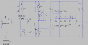
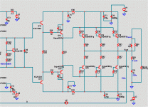
First the circuit -
1. Add 2.2R - 4.7R basestoppers to each output (covered in Bob's book).
Basestoppers on each driver , too. (22R - 47R)
2 . decouple both the current sources with the same resistive divider/cap (below 1) - minimizes "thump" (nearly eliminates it -both ccs's stabilize simultaneously)... Shown (below 1 -R9 ,10,22 and C5). Your call as far as what type CCS you want to use
.3. Look at my example as far as the input stage , the same adjustable CCS and offset control is used on about 50 amps now - it works very well.
The layout -
No problem with size and the coil (below 2 - inductor) sampson and all the OEM pro amp's put it in the same place. Saki's recommendation of local decoupling for the voltage stage is essential , either for common rail or boosted rail.
Your NPN Vbe to-126 device must be on the main heatsink to work. Just had had to let you know ..
.OS
Attachments
PICKY , PICKY ....
Most OEM output boards are large ... and for a reason...
You must spread the heat. The sampson above is 100mm X 200mm , most of the 3-4pair DIY EBAY boards are 75 X 175-200mm. To put 3-5 pair OP's on a 125mm board would be folly.
If you want a project to inspire , try Roender's thread - http://www.diyaudio.com/forums/solid-state/111756-rmi-fc100-single-stage-audio-power-amplifier.html
Larger board , all aspects covered.
OS
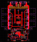
Went back and added base stoppers, next up will be some added decoupling for the boosted front end. Something like 100uF//100nF pr. rail should be good enough.
As for the Vbe TO-126 device, my plan was to mount it on top of one of the output transistors for faster reaction to thermal changes.
As for decoupling of the CCS's I wont bother with it, Im going to make a DC speaker protection with turn on mute etc. so even if theres is a turn on thump I wont notice it anyway. But thanks for the suggestion, maybe I'll add it or maybe I wont, dont really know.
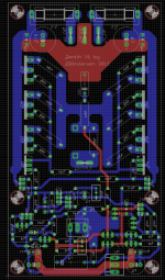
...... Have spent ,few hours, to layout schematic from first page , so the result attach ......
Alex.
alex without trying to make you feel uncomfortable and knowing very well that a pcb like that is a result of work of quite a few hours
there is a few thiongs that i dont like
1- all your pcb look the same
2- small ground frame is not really sure that works properly
3- more rounding in some areas is needed
4- feedback rooting is quite long
second PCB revised ......
..... Hi Sakis , nice to see you around here , thanks for comments .
I think it's your problem if you dont like my PCB's , I'm an poor diy guy who try to help this forum members .I'm not professional , not my job but I like to help others . I'm still learning something from here , a lot of good
thinks , informations . Second PCB ...
Alex.
.....
Hi Sakis , nice to see you around here , thanks for comments . I think it's your problem if you dont like my PCB's , I'm an poor diy guy who try to help this forum members .I'm not professional , not my job but I like to help others . I'm still learning something from here , a lot of good
thinks , informations . Second PCB ...
Alex.
Attachments
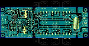
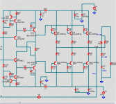
Took a while to change my layout but I managed it.
Base stoppers for drivers/outputs added and 100uF//100nF decoupling for the front end supply rails has been added.
Unless I get a bright idea sometime between now and Friday this is most likely what Im going with
Base stoppers for drivers/outputs added and 100uF//100nF decoupling for the front end supply rails has been added.
Unless I get a bright idea sometime between now and Friday this is most likely what Im going with
Attachments
Last edited:
ok ... we are getting somewhere ... i like it !!!! ha ha ha ...
one question only do you think that 2W emmiter resistor is enough ? i dont ...unless your outputs are super matched .... you may as well redesign for 2 per transistor ... or go for 5W each and place them diagonal like Jan does in the lynx pcb
other than that i think is perfect !!!
edit: small detail and easy to fix ... the traces that supply the base of outputs are in parallel and too close with the output .... brake them and do something like \_/\_/ that
Last edited:
#13 has no Vbe thermally coupled.
OS
Yes, but will most likely be attached on top of one of the output transistors.
Alex mm
I like a lot your compact layouted boards, they look great but you always pick some not so very good sch to my opinion. I suggest you to layout Mongrel sch on one board similar to this one, I'm sure Osty won't have anything against.
P.S. And guys pls use cascodes in schs in every possible places.
.....
I think it's your problem if you dont like my PCB's , I'm an poor diy guy who try to help this forum members .I'm not professional , not my job but I like to help others . I'm still learning something from here , a lot of good
thinks , informations . Second PCB ...
Alex.
I like a lot your compact layouted boards, they look great but you always pick some not so very good sch to my opinion. I suggest you to layout Mongrel sch on one board similar to this one, I'm sure Osty won't have anything against.
P.S. And guys pls use cascodes in schs in every possible places.
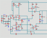
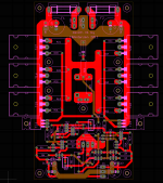
Decided to incorporate some of Ostrippers ideas :
Decoupling of both current sources with the same resistor/divider cap.
Trimpot offset control.
Base stoppers for all output pre/driver/output transistors. 62R/22R/2R2
As both Sakis and Ostripper suggested, decoupling for the IPS supply.
Lastly changed it to a triple EF and even managed to fit 3 pairs of OP transistors, although they are now NJW3281/1302. Alot cheaper than and almost as good as MJL4281/MJL4302.
Attachments
Last edited:
Careful with the triple !!! I have built both examples (below 1-2). A triple is VERY picky as far as layout and basestopper choices are concerned.
#1 - the standard triple
Q12-13 have NO stoppers - this seems to be essential for a stable gain stage.
Q14-15 have 10R stoppers (covered by Bob's book) the capacitive "stoppers" (C1/8) quench parasitic oscillations at clipping .... harmon kardon,luxman, and many others all use this technique. Note the R/C before driver/pre (R30/32 - C11/15).
OP's are standard (like a EF2) with 2R2 stoppers. Drivers and Op's are heatsinked
predrivers can be 2n5551 type or ksa1381 (to92 or to-126) and not heatsinked. You must compensate for about 5-6 Vbe's with this circuit.
#2- the DBT. Looks complicated but has better thermal tracking and less distortion. Same stopper choices but with the added CCS's. Driver and predriver are on the same small heatsink , all bolted together... they cancel out entirely. Just the OP's Vbe is compensated for. A simple 1:1 single transistor Vbe is all that is needed.
The reason for a triple is to minimize the load on the VAS. You can now run smaller VAS devices (MPSA92/94) at 3-4ma , couple them "face to face" and miniaturize the whole IPS/voltage stage. Both circuits only load the VAS with <50uA , even to drive 1R loads !! Distortion also drops by a factor of 10 , as the VAS linearity is improved.
OS
Attachments
Last edited:
- Status
- This old topic is closed. If you want to reopen this topic, contact a moderator using the "Report Post" button.
- Home
- Amplifiers
- Solid State
- Layout critique