Hi all,
With the arrival of new USB interfacing options such as the Exa devices, hiface and musiland, I have decided to try and design a DAC board, mainly for educational reasons.
I already have a (breadboards) DAC around PCM2706, too ugly to show it here, which amazed me by actually making music, therefore I have the means of taking an I2S signal for testing the new DAC until the exa device becomes available.
Regarding the board I am trying to layout, the only interesting design details, not used in the datasheet, are the following two:
1. Dedicated (digital and analogic) low noise IC: LT 1763. I intend to replace these with some other ones: LP5900, (6uV vs 20uV RMS noise figures) selected with the help of glt, our diyaudio member behind hifiduino. The reason for not using them from the start is that they need an even smaller, more difficult to solder package, and I am not ready for this yet.")
2. Inductors placed on each rail, between the decoupling capacitors. I've chosen for this some 805 pads, not sure if I can find something usefull at this size.
Question 1: I've used a single voltage regulator for both AVSS and Vref, do you believe I should treat these differently? Should the AVSS have a more advanced regulator (Buffalo dac uses some op-amps regulators if I recall correctly). And should I use separate regulators for AVSS and Vref, or this is not recommended?
Question 2: Can you please recommend some good beads for the decoupling parts? I really don;t know what characteristics these inductors should have.
Layout goals:
The routing done above is not the final one, and is not very well thought about. In fact is just for having something to upload and start with. I've done only to route the input wires, to make sure they stay on the top plane and then hit the autorouter.
I plan to:
- keep all the signal wires (except the control ones, which I am not sure I need them), on the top plane.
- pour a groundplane on the top. The high frequency signal wires should be separated by parts of the groundplane.
- pour a bottom power plane, at least across some parts of the PCB, and connect this with the top parts with vias.
Question 3: I've managed to place the decoupling capacitors prety close to the power pins, should I make an extra efforts and place some of the components (the inductors for example) on the bottom plane for even smaller distances?
Question 4: How do I pour a plane in Eagle? I used the polygon tool, and gave the polygon the same name (GND) with the net I was interested to connect with, using the tool name. I selected an Isolate value of 0,01. However the plane just won't render, as you can see in the above image. Any ideas?
Any other suggestions are welcomed!
With the arrival of new USB interfacing options such as the Exa devices, hiface and musiland, I have decided to try and design a DAC board, mainly for educational reasons.
I already have a (breadboards) DAC around PCM2706, too ugly to show it here, which amazed me by actually making music, therefore I have the means of taking an I2S signal for testing the new DAC until the exa device becomes available.
An externally hosted image should be here but it was not working when we last tested it.
Regarding the board I am trying to layout, the only interesting design details, not used in the datasheet, are the following two:
1. Dedicated (digital and analogic) low noise IC: LT 1763. I intend to replace these with some other ones: LP5900, (6uV vs 20uV RMS noise figures) selected with the help of glt, our diyaudio member behind hifiduino. The reason for not using them from the start is that they need an even smaller, more difficult to solder package, and I am not ready for this yet.
2. Inductors placed on each rail, between the decoupling capacitors. I've chosen for this some 805 pads, not sure if I can find something usefull at this size.
Question 1: I've used a single voltage regulator for both AVSS and Vref, do you believe I should treat these differently? Should the AVSS have a more advanced regulator (Buffalo dac uses some op-amps regulators if I recall correctly). And should I use separate regulators for AVSS and Vref, or this is not recommended?
Question 2: Can you please recommend some good beads for the decoupling parts? I really don;t know what characteristics these inductors should have.
An externally hosted image should be here but it was not working when we last tested it.
Layout goals:
The routing done above is not the final one, and is not very well thought about. In fact is just for having something to upload and start with. I've done only to route the input wires, to make sure they stay on the top plane and then hit the autorouter.
I plan to:
- keep all the signal wires (except the control ones, which I am not sure I need them), on the top plane.
- pour a groundplane on the top. The high frequency signal wires should be separated by parts of the groundplane.
- pour a bottom power plane, at least across some parts of the PCB, and connect this with the top parts with vias.
Question 3: I've managed to place the decoupling capacitors prety close to the power pins, should I make an extra efforts and place some of the components (the inductors for example) on the bottom plane for even smaller distances?
Question 4: How do I pour a plane in Eagle? I used the polygon tool, and gave the polygon the same name (GND) with the net I was interested to connect with, using the tool name. I selected an Isolate value of 0,01. However the plane just won't render, as you can see in the above image. Any ideas?
Any other suggestions are welcomed!
Last edited:
Just a short folow-up, I've managed to resolve the issue of polygon pouring, it seems that, eh, I was not hitting ratsnest button after pouring. The only tutorial in which I found this recommendation was HERE. It has a wealth of good info, regarding planes in eagle.
I've also made some changes on the board layout, but it's far from over. I gave more importance to the digital inputs and the analog outputs as you can see, but the digital control lines are snaking around the board in the left side and I don;t like that.
Also I'll digg in the datasheet to make sure I need all that control. As far as I can remember the dac automatically sets the fs by looking at the ratio between the lrclk and bitclock, so those lines probably won't be needed, except diff0 and diff1.
The priority is however optimizing the power lines on the bottom layer, and I was wondering if it would be ok to split the plane in three: VBUS, for the unregulated power line feeding the regulators, vreg 1 and vreg2 for the regulated lines that feed the decoupling capacitors for AVSS and DVSS.
An externally hosted image should be here but it was not working when we last tested it.
It seems rather quite around here, so I'll jump in some additional info. First of all I've noticed a huge layout problem around c11 and l3, the live track is surrounding all those components instead of taking the short route. However, I will proceed as on Tent's article on decoupling:
- The L bead will be as close as possible to the input dc pin.
- The unpolarized C will be as close as possible to the ground pin.
- Ground plane on the top surface.
- No power planes whatsoever, as they act as antennas according to Mr. Tent
Question: With the power plane out, there's a lot of room left on the bottom plane, would another ground plane hurt anything? Will some kind of parasitic capacitance occur between the two? I plan to place lots of vias between them if I proceed that way. What do you think?
Hi, For someone attempting to design a pcb he should already know the
basics and as you have identified some faults you should go ahead and
redo the pcb.Asking if one should use another ground plane when you know
in electrical theory even two trace side by side will create a capacitance is
asking a silly question.Solve problems when you encounter them,then you will
learn along the way.After all this is suppose to be to be educational right? So
keep it simple and you will probably succeed. singa
I would have a look at this, it shows how digital signals couple with the ground plane. I would route the board with the bottom layer as near a full ground as possible, ie minimise track and slots on that layer. Further more I would not route any signals over any slots in the ground plane.
I would also cover as much of the board as possible with ground pours, if they are tied together with vias they aint gonna cause a problem.
I would be interested in Mr Tents articles on power planes and de-coupling!
I would also cover as much of the board as possible with ground pours, if they are tied together with vias they aint gonna cause a problem.
I would be interested in Mr Tents articles on power planes and de-coupling!
From recent personal experience I can say that having a ground plane directly beneath the DAC chip on the copper top was required for distortion performance.
The main ground plane is the copper bottom and is completely uninterrupted, however on it's own, it wasn't enough, without the copper directly beneath the chip on the copper top, performance was significantly degraded. We're talking going from 0.02% to 0.0008% @ 192khz, or 0.002% to 0.0005% @ 48khz.
Marce, it looks like you intended on providing a link with your previous post?
Edit - SunRa, have you tried printing out the design and checking to see if the printer can resolve the fine separation between the tracks on the DAC chip? With Eagles default package size the printer I've got joined them all together, I had to resize the pads for it to work well. For SSOP packages I use 0.38mm width pads.
Last edited:
Hello,
Thank you all for your feedback, it's much appreciated.
Thanks singa for your input. To be honest this is my first real attempt of designing a PCB in eagle. All the PCBs I made in the past were based solely on high-end hardware (ruler and millimetric graph paper ). And actually this is the first one to have inputs in the MHz range.
However looking at some pcb designs that were made with RF in mind, I observed that they actually employ a double ground plane, therefore I decided to do that to. On the renderings below you can't see the via's though, because I hadn't place them yet. I plan to use many of them in order to minimize any capacitance that might occur.
Thanks for the advice, I try to do just that! By the way, any reason for keeping the Control Data Input Pin (DEM1 / CDTI) and Control Data Input Pin (CCLK / DEM0) connections? I plan not to make any changes in the registers and AK4396 is capable of automatically detecting the sampling rate so, any reason for keping those?
I tried to do just that regarding the ground plane. The bottom layer is mostly uninterrupted, and the top layer also has a fairly amount of ground plane.
Here is the link to Mr. Tent article.
Thanks for your reply 5th element. I did just that, both the bottom and the top graound planes are solid beneath the dac. However I just couldn't avoid using one via under the DAC for the PDN pin.
Thanks, I've missed that, in the next revision I will correct it!
edit: I've observed the renderings attached initially were at a low resolution so I've changed them and also connected pin 1 and 2
Followin the advice in Tent's paper, I removed the 0,1uf caps in the decoupling scheme and introduced L beads. The 10uF decoupling caps I am going to use are high quality OSCON's , with a low ESR, so no need for the small additional capacitance.
I did this for the VREF pins also. Now, there is this passage in the datasheet specifying that between VREFH and VREFL there is a 0,1uf cap. In the schematic there is another 10uF electrolytic in parallel. Any reason for the 0,1uF to be mandatory, or have any other purpose than decoupling?
I am making now the final steps for sending this to the fab so please let me know if there any further changes to be made.
Thanks!
Thank you all for your feedback, it's much appreciated.
Hi, For someone attempting to design a pcb he should already know the
basics and as you have identified some faults you should go ahead and
redo the pcb.Asking if one should use another ground plane when you know
in electrical theory even two trace side by side will create a capacitance is
asking a silly question.
Thanks singa for your input. To be honest this is my first real attempt of designing a PCB in eagle. All the PCBs I made in the past were based solely on high-end hardware (ruler and millimetric graph paper
). And actually this is the first one to have inputs in the MHz range.However looking at some pcb designs that were made with RF in mind, I observed that they actually employ a double ground plane, therefore I decided to do that to. On the renderings below you can't see the via's though, because I hadn't place them yet. I plan to use many of them in order to minimize any capacitance that might occur.
Solve problems when you encounter them,then you will
learn along the way.After all this is suppose to be to be educational right? So
keep it simple and you will probably succeed.
Thanks for the advice, I try to do just that! By the way, any reason for keeping the Control Data Input Pin (DEM1 / CDTI) and Control Data Input Pin (CCLK / DEM0) connections? I plan not to make any changes in the registers and AK4396 is capable of automatically detecting the sampling rate so, any reason for keping those?
I would also cover as much of the board as possible with ground pours, if they are tied together with vias they aint gonna cause a problem.
I would be interested in Mr Tents articles on power planes and de-coupling!
I tried to do just that regarding the ground plane. The bottom layer is mostly uninterrupted, and the top layer also has a fairly amount of ground plane.
Here is the link to Mr. Tent article.
From recent personal experience I can say that having a ground plane directly beneath the DAC chip on the copper top was required for distortion performance.
Thanks for your reply 5th element. I did just that, both the bottom and the top graound planes are solid beneath the dac. However I just couldn't avoid using one via under the DAC for the PDN pin.
The LT1763 need pin 1+2 tied (out+sense) together!
Thanks, I've missed that, in the next revision I will correct it!
edit: I've observed the renderings attached initially were at a low resolution so I've changed them and also connected pin 1 and 2
Followin the advice in Tent's paper, I removed the 0,1uf caps in the decoupling scheme and introduced L beads. The 10uF decoupling caps I am going to use are high quality OSCON's , with a low ESR, so no need for the small additional capacitance.
I did this for the VREF pins also. Now, there is this passage in the datasheet specifying that between VREFH and VREFL there is a 0,1uf cap. In the schematic there is another 10uF electrolytic in parallel. Any reason for the 0,1uF to be mandatory, or have any other purpose than decoupling?
I am making now the final steps for sending this to the fab so please let me know if there any further changes to be made.
An externally hosted image should be here but it was not working when we last tested it.
An externally hosted image should be here but it was not working when we last tested it.
An externally hosted image should be here but it was not working when we last tested it.
Thanks!
Last edited:
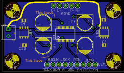
The trace on the copper bottom that splits the ground plane pretty much straight down the middle, move this trace, unless this is by design.
You've also got a few traces on the copper bottom that really don't need to be there, unless these are by design too, move them to the copper top instead.
In the attached image you can see where I chose to route the trace that splits the ground plane in half. Only you could also do the exact same thing on the copper top instead.
I've pointed to two specific traces, but those could be on the copper top too. In fact I'd have thought you could put all the traces that are on the bottom onto the top.
Place a small resistor in series with each clock line going into the DAC, a 47R or something will be fine.
Attachments
Thanks for the fast reply and the additional exemplification.
I tried to keep the power lines on the bottom plane, that was the main reason for routing like that. Routing the PDN and MCLK tracks was silly indeed, I thought I can get some extra shielding though.
Here's the new version, all tracks on the top plane. The bottom plane can be a ground shield or I can scrap it. If the fab tells me that it's much less expensive to make the board without the bottom plane and all the additional vias needed to connect the two grounds then I'll just scrap it.
What do you think? Is this a release candidate?
An externally hosted image should be here but it was not working when we last tested it.
Thanks for the help and suggestions. I still have to print the circuit on a paper and check if the pads and footprints are matching. Also I'll have to arrange the silk screen a bit. Then I'll contact a fab for quotation. Having no vias, I will also considering doing it in-house, with UV method.
Regarding the control clock and control data pins, dem0 and dem1 on the board, am I right that these are not really needed? I couldn't find much info regarding this in the datasheet, just some register stuff I can hardly understand right know.
Regarding the control clock and control data pins, dem0 and dem1 on the board, am I right that these are not really needed? I couldn't find much info regarding this in the datasheet, just some register stuff I can hardly understand right know.
Thanks, I was aware of that table and I am still trying to make my way through all the settings and configurations this DAC is able of.
However one feature I don't understand. The datasheet is continuously referring to serial and parallel mode (with PCM, not with DSD) and I couldn't find a definition regarding this. I assumed that parallel mode meant using two chips for dual mono mode but now I highly doubt it. Also I couldn't find a similar operation mode in other datasheets (for AD1955, PCM1794). Any insight on this? Are these two types of input data? I thought the I2S is pretty straightforward...
However one feature I don't understand. The datasheet is continuously referring to serial and parallel mode (with PCM, not with DSD) and I couldn't find a definition regarding this. I assumed that parallel mode meant using two chips for dual mono mode but now I highly doubt it. Also I couldn't find a similar operation mode in other datasheets (for AD1955, PCM1794). Any insight on this? Are these two types of input data? I thought the I2S is pretty straightforward...
Hi, Not quite yet.
You have laid out pcb in symetrical textbook fashion,visually nice to look at but I feel you can shorten some traces further.
Look at both pairs of oscons don't you think their traces can be shorter?
If you rotate the angled sides towards the dac respectively you can improve the proximity of the power lines to the dac.Now you send to the pcb fab.
PS you have an orphan ground pour (pad) near pin 18 of dac.This can potentially short the smt inductor if solder overflow and cause a power short which may be costly and not easy to spot so delete it.Also check the connections to ground pour connections of other components.
singa
Last edited:
Thanks, I was aware of that table and I am still trying to make my way through all the settings and configurations this DAC is able of.
However one feature I don't understand. The datasheet is continuously referring to serial and parallel mode (with PCM, not with DSD) and I couldn't find a definition regarding this. I assumed that parallel mode meant using two chips for dual mono mode but now I highly doubt it. Also I couldn't find a similar operation mode in other datasheets (for AD1955, PCM1794). Any insight on this? Are these two types of input data? I thought the I2S is pretty straightforward...
Hi SunRa,
In AKM terminology, serial means the DAC is controlled in software mode using SPI or I2C control. Parallel means the DAC is hardware controlled.
Regards
unixdeveloper
Hi SunRa,
In AKM terminology, serial means the DAC is controlled in software mode using SPI or I2C control. Parallel means the DAC is hardware controlled.
Thanks, would you mind developing this a bit? In parallel mode the DAC is controlled by a a combination of the pins having specific functions, while in serial mode is controlled by a microcontroller?
If you rotate the angled sides towards the dac respectively you can improve the proximity of the power lines to the dac. Now you send to the pcb fab.
Thanks, it's a very good sugestion, I'll try it out.
PS you have an orphan ground pour (pad) near pin 18 of dac.This can potentially short the smt inductor if solder overflow and cause a power short which may be costly and not easy to spot so delete it.Also check the connections to ground pour connections of other components.
I've noticed that too (and it's not the only occurence, there are some others around the VR's) and I wanted to address is but I don't know how to erase that portion in Eagle. It's part of the polygon making the grounding plane, and I've tried working the "isolate" and "width" value with no success. Any sugestions?
- Status
- This old topic is closed. If you want to reopen this topic, contact a moderator using the "Report Post" button.
- Home
- Source & Line
- Digital Line Level
- New AK4396 DAC board design support needed