Hello.
I have been planning to build an amplifier based on the TI's TAS5630.
The EVM and all the designs in the internet I have seen seem to have the PVDD caps placed over the outputs. Is that necessary? I was thinking of feeding the chip from underneath and instead of four 1000uF caps, having two 2200uF caps [picture attached]. This would allow for a much easier design of the output side . I heard the 2,2uF ceramic caps should be as close to the chip as possible, so I'll move them.
But does this sound like a good idea at all?
I'm going to run it in PBTL mode, ~180W at max.
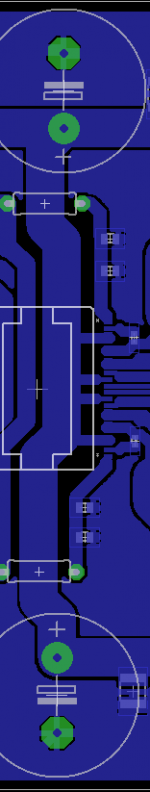
Attachments
I found with class d that layout and proximity of decoupling caps to be vital.
I had a 12v regulator 3 inches from the IC and the IC kept resetting at a high frequency. I found I had to decouple the 12 volts not only at the chip but close to the regulator too.
I also had trouble with tyhe B+, GND and B- decoupling, i found these had to be close to the output MOSFETs.
Class d can be a real pain to get right.
If you have seen a layout tha tworks then use it.
It can get expensive if you need 2-3 iterations of pcb before it works.
The EVM and all the designs in the internet I have seen seem to have the PVDD caps placed over the outputs. Is that necessary? I was thinking of feeding the chip from underneath
From my experience, two most important rules for this chip are to have the continuous groundplane (having all GND points connected to this groundplane directly using vias) and to have the PVDD caps placed as near as possible...
- Status
- This old topic is closed. If you want to reopen this topic, contact a moderator using the "Report Post" button.