Hi All,
a very interesting conversation after work ended up in me missing dinner but having half thrashed out a really novel chassis design.
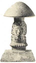
The main part, apart from the hemi-spherical perspex cover, is a mushroom-shaped pcb. I appreciate that I could produce my own boards and cut them to shape, but does anyone have any experience of having wacky shaper PCBs professionally produced??
All the best
Jon
If you mean 3D boards, there are two basic methods used commercially. One is to make a flex board, then cut and shape it. This is relatively easy to do, but not cheap. The other is to make true molded boards, which sounds like what you're asking about. That's a process which is reasonable in production, but hideously expensive for one-offs.
In theory, you could use conductive paints and solderable conductive stakes for a DIY approach, but I haven't tried that myself.
In theory, you could use conductive paints and solderable conductive stakes for a DIY approach, but I haven't tried that myself.
Mushrooms etc.......
Thanks for the pointers. The PCB is actually a semi-circle with a tab on the bottom - mounts vertically in the chassis. The hemi-sphere goes over the whole lot, a little like those antique mantlepiece clocks with the spinning ball mechanism.
Thanks again
Jon
The PCB shape would be thus:
Thanks for the pointers. The PCB is actually a semi-circle with a tab on the bottom - mounts vertically in the chassis. The hemi-sphere goes over the whole lot, a little like those antique mantlepiece clocks with the spinning ball mechanism.
Thanks again
Jon
The PCB shape would be thus:
Attachments
Decent PCB houses in the UK...
Hi John,
at the risk of hijacking my own thread, which would you recommend? I would prefer a top quality service for bottom drawer money!!!!!
 I will prototype the boards myself, though, just to make sure the units actually worked and sounded nice!
Haven't built anything yet, tho' (what a fraud!!!) !
!
Jon
Hi John,
at the risk of hijacking my own thread, which would you recommend? I would prefer a top quality service for bottom drawer money!!!!!
 I will prototype the boards myself, though, just to make sure the units actually worked and sounded nice!
Haven't built anything yet, tho' (what a fraud!!!)
Jon
Jon,
This is the one that I've used for about 2 years now:
http://www.bpc-circuits.co.uk/welcome.htm
I'm a small customer, but they treat me well.
You need some lingo and basics if you've never dealt with a board house:
PTH: Plate through hole; All multi-layer boards use these.
Layers: Houses usually include any legend, or silk-screens as separate layers. Also solder masks are considered as layers. Most multi-layer designs can use a common solder mask for top and bottom.
More than 2 copper layers causes the price to hike, as boards must be laminated.
Even if you want 5 or 10 of a small board, it's best to have them done as a single prototype, and cut to separate. This depends upon the size of raw board the house works with.
The House will require a Gerber (plot) file for each layer, and a drill file. Exceptionally, houses will accept the native .pcb file and extract it for you.
If extracting your own files, they MUST have the same time stamp.
There are some economy houses that require files of proprietry format. These are cheap, but they'll mix your work with others, and so can't cater for special requests.
Hhhh,
Cheers,
Cheers,
Board Houses
Hi John,
thanks for the information - very helpful indeed. My chassis concept is based on a common design with the different pcbs as plug-in modules. For instance, a pre-amp would consist of a pwr supply board back to back with a pre-amp board, and both mounted on a single drop-in caddy. Likewise, for instance, the GC module would comprise a rectifier board and amp board. The possibilities are endless: an active x-over with pwr supply, DAC with pwr supply. All ac secondary voltage is supplied by wall warts or toroids in a separate casing.
When I get some time, I am going to draw the design up properly and try to work out how much each chassis is going to cost.
Don't hold your breath, but you saw it here first!!!!!
All the best
Jon
PCB Software
Hi John,
I've got Eagle and ExpressPCB. I'm just playing with them at the moment. When I have finished the course I'm on,, I'll look at them in more detail. The learning curve does appear to be a little steep! Any others that you might recommend??
Is schematic capture different from laying out a line diagram (for instance copied from a datasheet etc)?
Cheers
Jon

Jon,
"Schematic capture" is just a name given by some of the PCB software vendors to describe the transition from a schematic into a PCB. This normally produces a "rats nest" where the nets are connected by the shortest routes, and without layer. Then it's up to you to push them around manually, or use an auto-router.
You should be informed that the most time consuming task of all this it library management. Each schematic symbol can be associated to one or more PCB-component symbols. All software packages have librarys of common components, but there are ALWAYS components that you have to create yourself. On the Eagle site I remember that there is an area for sharing librarys.
The software I use myself is paid for, and mid priced. I think it is outside the budget of DIY. This kind of software costs between £100 and £5000. Mine is in the middle.
You are probably best to stick to Eagle. It's the best non-proprietry-file package IMO.
Cheers,
Thanks John....
Eagle it is, then!
I have briefly looked at trying to create the LM3875 in Eagle, but I quickly realised that it was going to be a more complex task than it first appeared. I will have another go when I have the time to really look into it in some depth.
Their Burr Brown (and other) libraries are really quite comprehensive though - which is a boon.
Thanks for the pointers.
Jon
- Status
- This old topic is closed. If you want to reopen this topic, contact a moderator using the "Report Post" button.
- Home
- General Interest
- Everything Else
- Shaped PCBs

