I started to build a battery-powered, JFET-based phono stage mid last year. The circuit was sent to me by a friend of mine who said it really sounded great ... so I thought I may as well try it out, to see whether it bettered my own phono stage. So I built it and listened to it ... yes, it sounded very nice but, when I measured its RIAA equalisation (using a sig-gen fed through a Hagerman reverse RIAA board), the 20hz reading was low by over 4dB.
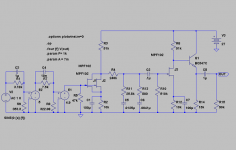
This phono stage uses:
* a pair of JFETs as the input stage, followed by
* a passive composite RIAA network, then
* another JFET gain stage, followed by
* a transistor output buffer (unity gain).
Schematic attached.
I found that the values of the components in the passive composite RIAA equalisation network do not match the values obtained from using the equations in this most interesting article:
Phono Stage Design
So I wanted to correct the values. I have subsequently twice rebuilt the RIAA equalisation circuit so that it matches the equations (each time making some different assumptions) and still can't get it to measure any better.
So I thought I would ask here for help from anyone who knows their JFET theory.
The first question I would like an answer to is this:
* the attached article shows that R1' (which is the value obtained by R0 (240K in the schematic) & R1 (510K) in parallel) is the basis for generating all the passive RIAA network component values.
* however, I was told that you have to add the Zout of the input JFET stage to R0, to get the right calculation for R1'.
Is this correct?
My second question is:
* is it true that the Drain resistor of the input JFET pair defines their Zout?
I appreciate that in the circuit shown, the Drain resistor value is equal to the source resistor value (so it doesn't matter) but, in my circuit the Source resistor is much lower (because I've used a DC rail using 5x6v SLAs = 30v, not 3x9v transistor batteries = 27v).
All I know is, when I calulated R1' by taking 291K & 510K in parallel and then generated all the RIAA values using the equations in the attached paper, it didn't measure any better than the original circuit.
So I'm wondering if the Zout of the input JFET pair is in fact equal to something else than 51K?
Thanks,
Andy
Attachments
This data sheet:
http://www.onsemi.com/pub_link/Collateral/MPF102-D.PDF
shows the reverse transadmittance is about 0.01 mmhos ie 100k
Two in parallel is 50K, so the RIAA network is loaded down at low frequencies
This device is intended for rf work and is badly controlled for audio applications like this eg the decade range of Idss
As mjf says the major problem is the coupling cap that is both wrong value and also wrong placed.
This is an example of a +/-0,1dB correction with the 4th time-constant added. Unfortunately there is to low current through the FETs. Adjust the source-resistor to get Ud just above 10V.
This is an example of a +/-0,1dB correction with the 4th time-constant added. Unfortunately there is to low current through the FETs. Adjust the source-resistor to get Ud just above 10V.
Attachments
As said - I've seen the MPF102 used as RF amplifier several times, but never on audio. 2SK170 would be a much better choice....
Also - the inverse RIAA ciruit being fully passive, expects a 47k load -not 51k. This will affect the readings somewhat (without doing the calculations). It also assumes your test generator have an output impedance of 50 ohms. Not all of them have, and some are switchable. How about yours?
Also - the inverse RIAA ciruit being fully passive, expects a 47k load -not 51k. This will affect the readings somewhat (without doing the calculations). It also assumes your test generator have an output impedance of 50 ohms. Not all of them have, and some are switchable. How about yours?
Hey AuroraB,
47k or 51k doesn´t matter that much even if it will give some small deviations. The correction together with the malplaced and to small couplingcap is the major source of trouble.
The one I show above is fed via a corrected version of Hagermans theoretical rev-RIAA. Unfortunately he made a mistake in his article which he admitted when I contacted him. His commercial revRIAA is correct though. But as you say it must be fed with the correct source and loaded right.
The FETs run at about 150uA each and that isn´t optimal in my eyes. SK170 at 5-8mA would be a far better choice.
This data sheet:
http://www.onsemi.com/pub_link/Collateral/MPF102-D.PDF
shows the reverse transadmittance is about 0.01 mmhos ie 100k
Two in parallel is 50K, so the RIAA network is loaded down at low frequencies
This device is intended for rf work and is badly controlled for audio applications like this eg the decade range of Idss
Hi David,
Sorry, I don't have too much knowledge about this ... are you saying that the MPF102 is the wrong JFET to use and I should replace it with one that's designed for audio frequencies?
Like the SK170 which revintage suggests or the 2SK170 which AuroraB suggests, in threads further down?
Thanks,
Andy
hello.
if i read correctly there is a 0,01uf poly cap between the drains of the first stage and the 240k res........this cap is a little bit small, i think it cuts off the bass.
have you tried out to make it a little bigger........may say 47nf or 100nf?
greets
Thanks, mjf.
Yes, I had been told before that the input cap to the RIAA network was a bit low ... so I doubled it. But it seems I should've "ten-times'd" it!
But, given that the phono stage output coupling cap is 1uF, can you explain why 100nF will be sufficient for this cap after the input pair of JFETs - ie. if 100nF is good, would 470nF be sonically better?
Thanks,
Andrew
You didn't specify the signal generator used. If you are using a sound card, the output impedance may be too high. I had to buffer mine to get it to work properly with the reverse RIAA network
Sheldon
I'm using a 'real' signal generator that I bought from an electronics hobbyist shop a decade ago. But this is run through the Hagerman reverse RIAA board into the phono stage - so I'm assuming that its Zout is fine?.
Thanks,
Andy
There is one more major flaw in this design. THD will will surely be around 1% at nominal 5mV input. Typical FETs must be loaded harder with some local NFB to work acceptable.
Remember FETs aren´t the most linear devices.
2SK170=SK170, just was to lazy to add the prefix. Two paralleled with unbypassed source resistors at a total of 10-15mA(ca 10V Ud) will fix it. Also the second stage will need fixing as this is the major contributor to the high THD.
Still if you follow the RIAA correction in my schematic you will be close to correct. Just minor adjustments needed to get it right IRL.
But THD will unfortunately ruin it anyway.
Last edited:
Q:Yes, I had been told before that the input cap to the RIAA network was a bit low ... so I doubled it. But it seems I should've "ten-times'd" it!
.....0,01uf = 10nf........x 10 = 100nf,it was a suggestion to begin with.
you can use bigger caps in both positions if you want.smaller caps have a higher impedance at deep tones and cut them off if the load res is too low(e.g. low input impedance of the following preamp).
Q:But, given that the phono stage output coupling cap is 1uF, can you explain why 100nF will be sufficient for this cap after the input pair of JFETs - ie. if 100nF is good, would 470nF be sonically better?
......yes ,this can happen - but a smaller cap acts as a rumble filter,so this is not always a bad thing,you have to decide for yourself what you want(personally preferences).
greetings
Last edited:
The difference between rf and audio parts is the testing and binning by the manufacturer. For audio applications with no negative feedback you are interested in a narrow spread of Idss and gm to allow you to match left and right channel gainHi David,
Sorry, I don't have too much knowledge about this ... are you saying that the MPF102 is the wrong JFET to use and I should replace it with one that's designed for audio frequencies?
Like the SK170 which revintage suggests or the 2SK170 which AuroraB suggests, in threads further down?
Thanks,
Andy
The difference between rf and audio parts is the testing and binning by the manufacturer. For audio applications with no negative feedback you are interested in a narrow spread of Idss and gm to allow you to match left and right channel gain
Thanks, David ... but you've been a bit too cryptic for me.
OK, "for audio applications with no negative feedback you are interested in a narrow spread of Idss and gm to allow you to match left and right channel gain". Does this mean the MPF102 (described by posters as for RF) or the SK170 is best for my phono stage?
Regards,
Andy
As mjf says the major problem is the coupling cap that is both wrong value and also wrong placed.
This is an example of a +/-0,1dB correction with the 4th time-constant added. Unfortunately there is to low current through the FETs. Adjust the source-resistor to get Ud just above 10V.
Thank you very much Lars. I presume you used some simulation software to come up with these RIAA component values? With your help, it seems I might finally be able to get this damn phono stage to work properly
but you have raised some Qs in my mind. So if you could answer the following, I'd be extremely grateful:Q1. According to the equations for a passive composite RIAA circuit given in the paper that I referenced in my original post:
Phono Stage Design
C1 (12.5nF in your schematic) is calculated by this equation:
(a) R1' x C1 = 2187 x 10^-6
If I calculate R1' by taking R0 || R1 - ie. 240K || 510K - I get 163K.2 ohms
If I use this value in equation (a) above ... I get C1 = 13.4nF
Your simulation program got 12.5nF ... which implies that R1' = 175K.
Doing the calculation to find out what the value of R0 must be (if, in parallel with 510K, we get 175K) ... I get 266,418 ohms. IE. 240K + 26,418 ohms.
So where does this value of 26K come from?
Is it in fact the output impedance of the input pair of JFETs?Q2. C2 is calculated by this equation:
(NB: This is the C2 in the referenced paper - not the C2 in your schematic!)
(b) R1' x C2 = 750 x 10^-6
With R1' = 175K, I get 4.49nF ... whereas your simulation program has C2 = 4.1nF?
So why the difference?
Q3. The (series) coupling cap called 'C2' in your schematic has been moved from the Drain of the input pair of JFETs to just before the 510K resistor.
I'm curious to know why it is best located there (which is still within the RIAA equalisation network) ... instead of after the 510K resistor, at the input to the following JFET?
BTW, yes, I had picked up that there is far too little current flowing in the input pair of JFETs. So I reduced their Source resistor from 51K down to about 13K5, which meant that the Drain-Ground voltage was about half supply (I used a 30v supply, with 5x6v SLAs, instead of 27v).
Thanks,
Andy
hello.
may i show you an example of a wellknown phono pre that uses fet's and a passive eq. network.........the pearl phono from passlabs - year 2001
Pass DIY: Articles/Projects
........a fet needs a connection (mostly it is a res) from gate to source(or ground).....if you build in a cap between gate and (gate)res this will not work("no biasing").
greetings
hello.
may i show you an example of a wellknown phono pre that uses fets and a passive eq. network.........the pearl phono from passlabs - year 2001
Pass DIY: Articles/Projects
........a fet needs a connection (mostly it is a res) from gate to source (or ground).....if you build in a cap between gate and (gate) res this will not work("no biasing").
greetings
Ah, thank you, mjf. Right, so the 510K res needs to be directly attached to the Gate of the JFET which follows the composite RIAA network.
Can you explain (for my education!
) what is wrong with the original position of the series coupling cap (0.01uF) - off the Drains of the input JFET pair? (Circuit schematic attached for your convenience.)Regards,
Andy
Attachments
when I measured its RIAA equalisation (using a sig-gen fed through a Hagerman reverse RIAA board), the 20hz reading was low by over 4dB.
You didn't specify with what you measured the output signal with. If it was a computer soundcard you may have been dealing with 10k impedance. Together with the 1 uF output cap that would explain your -3dB at 20 Hz.
Can you explain (for my education! ) what is wrong with the original position of the series coupling cap (0.01uF) - off the Drains of the input JFET pair? (Circuit schematic attached for your convenience.)
...........only my opinion: from a technical point of view it is not really "wrong" if the cap is big enough that he does not affect the eq network.......but for convenience i would add this part onto the following stage,i think it is easier to handle/calculate.
greets
) what is wrong with the original position of the series coupling cap (0.01uF) - off the Drains of the input JFET pair? (Circuit schematic attached for your convenience.)...........only my opinion: from a technical point of view it is not really "wrong" if the cap is big enough that he does not affect the eq network.......but for convenience i would add this part onto the following stage,i think it is easier to handle/calculate.
greets
- Status
- This old topic is closed. If you want to reopen this topic, contact a moderator using the "Report Post" button.
- Home
- Source & Line
- Analogue Source
- Help requested from JFET-knowlegable people :-))