This is going to be quite a long post with lots of pictures so you've be warned.
It's taken too long to get to this! But I finally got some decent output inductors courtesy of Ice Components who were generous enough to supply me with 8 samples. From what I can tell these are the 17 series 10uH version, the 1D17B-100M.
They are relatively compact and come in a nice form factor for incorporating into PCBs. Here be a picture.
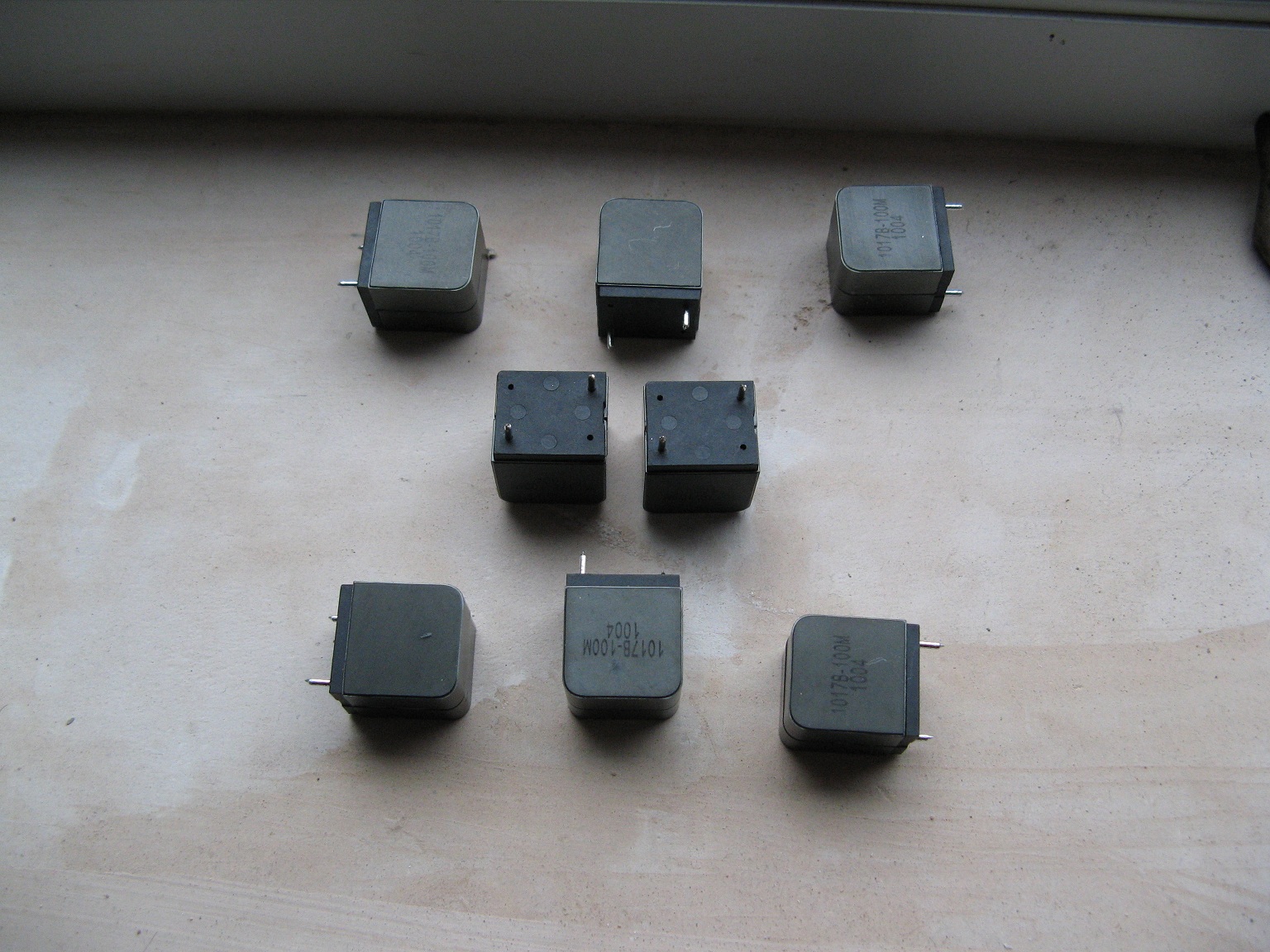
Unfortunately I didn't include anything as a reference for size, but you can see their dimensions here.
So without further ado I present you with a low quality picture with very poor lighting of the TAS5630 PCB + components on it's shelf. (No I've not made a case yet).
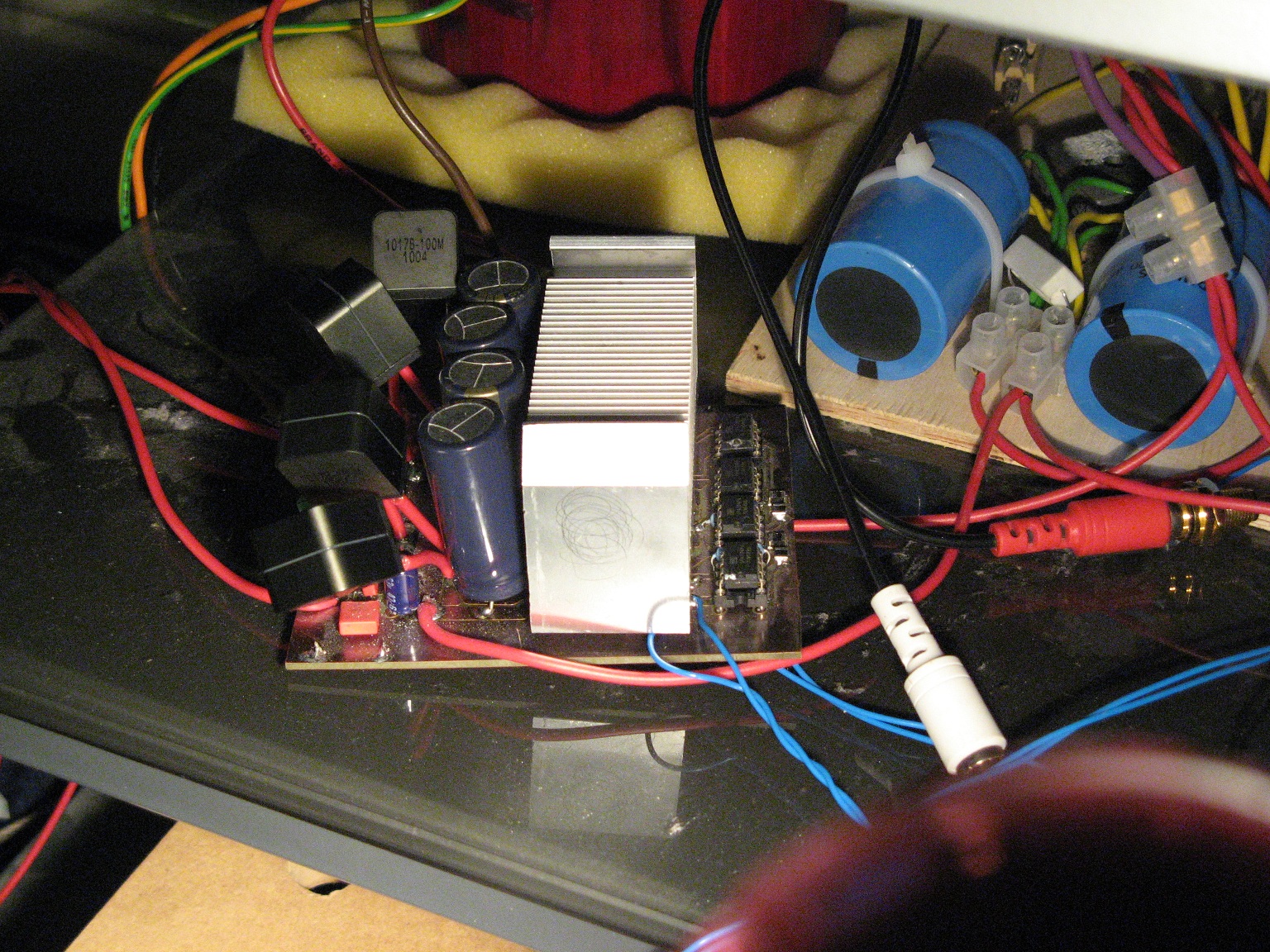
Here you can see the Ice inductors soldered in place on their little wire stilts. As you can see the entire PCB for the amp isn't very large at all.
The heat sink I chose to use was an old AMD cooler that I chopped in half. It looked like this...
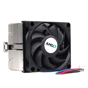
before I went at it with the hack saw. I chopped along the two slits that held the retainer clip and ended up with two nicely sized heat sinks.
I strapped a 17 watt power resistor two one of them and measured the performance at something like 4.5 degrees per watt without any fan cooling. With fan this decreased down to around 0.5 degrees per watt, which I found a little hard to believe. Either way, when the 5630s are idling the heat sinks get warm to the touch. The old inductors I had would get really hot at around 65 degrees centigrade, the Ice ones run much much cooler. You can barely even tell the amp is on, that's how cool they run. Changing inductors also had the knock on effect of placing less stress on the main chip as that runs cooler when idling as a result too.
Compared to the TI data sheet, I've changed the input opamps and their function and placed a 4th order high pass @ 20hz before the amp.
Before showing you any measurements, I'll first show how the system I used to measure the amplifier measured. In my gallery you can see measurements of the sound card alone. I wont post those here to save on cluttering up the post.
As the TAS5630 has a bridged output I needed some way of summing the +ve and -ve outputs together. This comprises of a simple opamp circuit with variable gain and DC blocking caps. I powered it off the +-12 volts lines used to power the opamps on the 5630s board.
Here's how the measurement system measured using the balanced outputs of the sound card to drive it.
Showing perfectly adequate results for measuring this amp.
Next are two scope pictures showing how the output filters affect the carrier frequency. The carrier wave simply looks like a messy square wave, it's peak to peak voltage spanning the +ve supply voltage on the Half bridges, which in this case is around 45 volts.
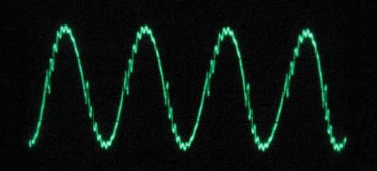
This is at 2 volts p-p showing the effect of the output filter on one side of the bridged output. If my arithmetic is correct this shows ~27dB of attenuation.
In bridged digital amplifiers TI allow you to use a function called BD modulation which they describe as.
BD modulation — modulation scheme developed to greatly reduce or eliminate the output filter. The
filter-free modulation scheme minimizes switching
current, which allows a speaker to be used as
the storage element in place of an LC filter and still lets the amplifier be very efficient.
The knock on effect of this is that you can cancel out some of the carrier frequency when the +ve and -ve outputs of the amplifier sum.
As a result we end up with...
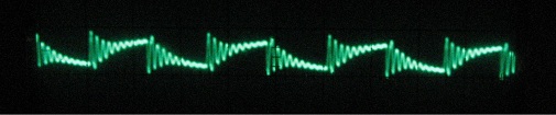
This shows a drop to 0.4 volts p-p, further increasing the attenuation of the carrier frequency up to ~41dB.
The power supply that I use isn't huge, which suits music fine, but under sine wave testing the power droops considerably under heavy load, thus reducing the max output power quite substantially.
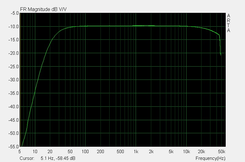
The first few graphs illustrate how the frequency response changes when the amp has different loads placed on it.
First up is unloaded.
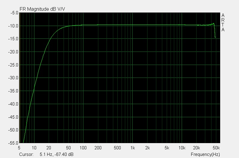
The measurement bandwidth limits exactly what you can see here. But you can easily see that there's going to be a small peak in the response at some point.
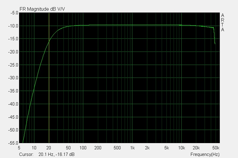
Next up the 9.4 ohm load.
The 4.7 ohm load
And the 2.35 ohm load
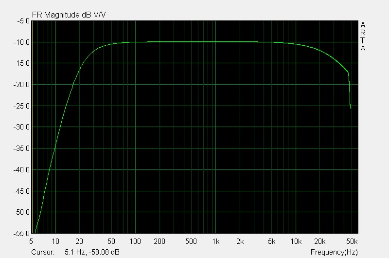
This clearly illustrates how sensitive the overall balance of a system will be when using a digital amp like this. And will require tuning based on the load. There are some schemes that include the output inductor within the feedback network and as a result they eliminate the FR variation based on load. This is clearly an area that TI might want to exploit if it's easy to implement.
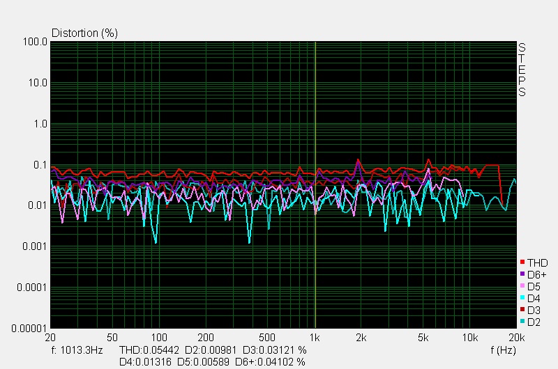
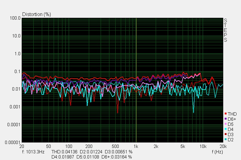
Now onto the distortion measurements. The first four are done into the 2.35 ohm load.
The first shows distortion at 2.5 volts p-p that represents what would be 0.1 watts into an 8 ohm load.
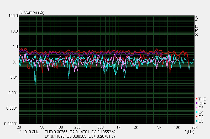
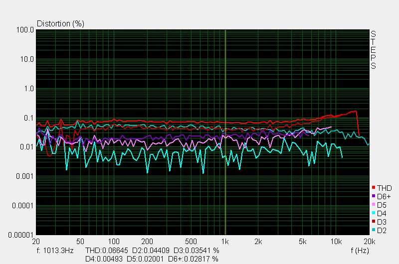
Next up is 8 volts p-p. What would be 1 watt into an 8 ohm load.
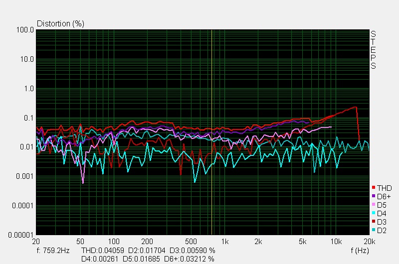
Next is 25 volts p-p, 10 watts into 8 ohms.
Each time you can notice the distortion going down as the S/N ratio is increased.
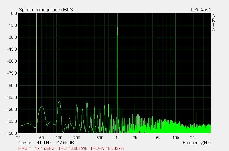
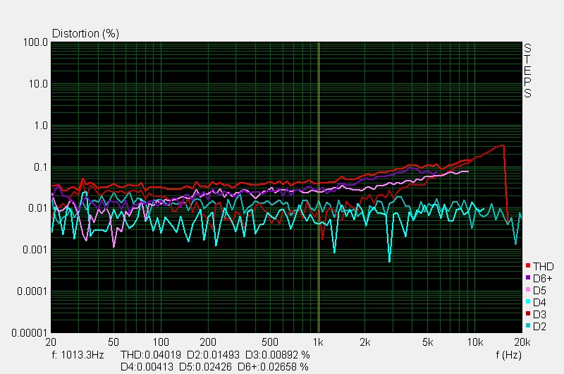
Here we've got 56 volts p-p, which is about the limit this PSU can get to before any clipping at all is shown as the voltage droops rather considerably. This represents 170 watts into the 2.35 ohm load,
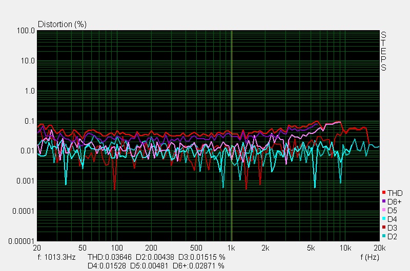
You can see that the distortion doesn't go down any further and that there's a slight rise in distortion towards higher frequencies. I wondered if this was a result of the inductors showing signs of reaching some kind of limit, so I ran a similar test into both my 4.7 and 9.4 test loads.
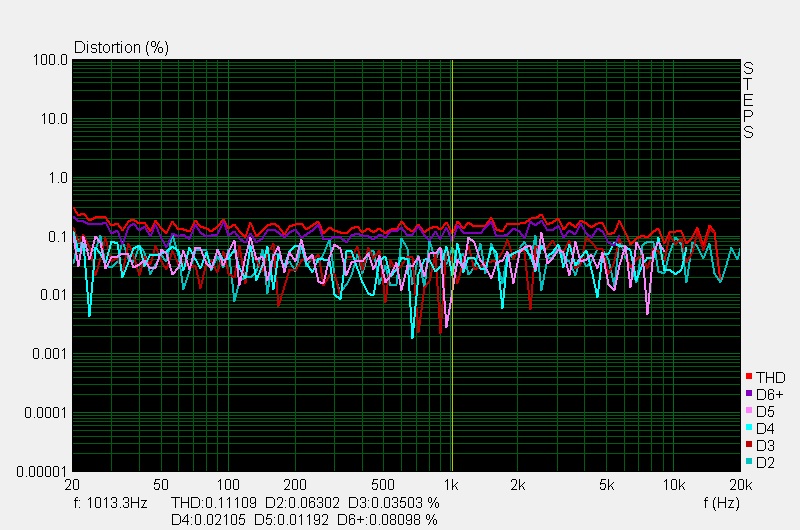
Here's 68 volts p-p into the 4.7 ohm load representing the maximum output this PSU could provide before any clipping, 124 watts. In this picture the distortion wobbles around a little too, this is from a very very mild amount of clipping.
Next 70 volts p-p into 9.4 ohms = 65 watts.
The same trend is evident, but it gets worse for decreasing load. This is probably due to the differing response of the output filter.
As a result of this I tried measuring the distortion at a much lower level into both the 4.7 and 9.4 ohm loads. First up is the 4.7 ohm load.
And now the 9.4 ohm load.
Again you can see the same similar trend towards high frequencies, with the easier load having the worst performance.
You can compare this to the 25 p-p graph into the 2.35 ohm load, that measures almost completely flat.
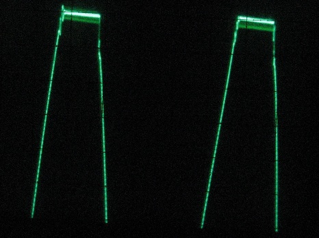
Next up some clipping.
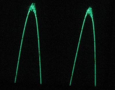
First is a graph of some very mild clipping @ 1khz showing the spectrum of the harmonics produced.
And next a scope picture of the same.
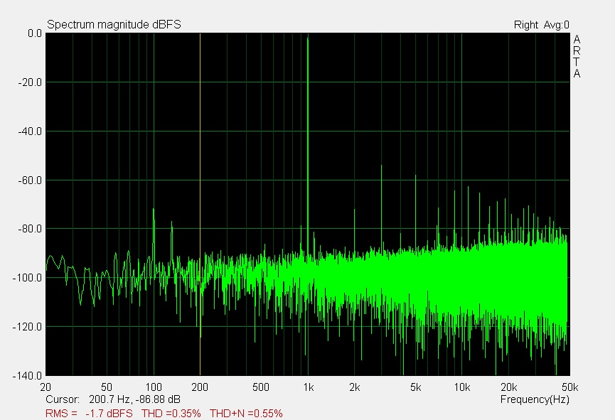
And now 9% THD.
The 0.35% you could perhaps live with, but the 9% looks utterly horrible. No one would ever want to listen to anything with that going on, at least not if they didn't want to get a headache. Quite why TI quote the power level at 10% THD I don't know as it isn't really representative of any real world situation. Most people would turn it down if it got to that point.
That's basically it as far as my measurements went.
In conclusion I can say that the Ice Components inductors didn't appear to break a sweat in the least. The overall performance being roughly what TI state for the PBTL mode as being around 0.05%. The increase in distortion towards high frequencies doesn't appear to be related to the inductors, otherwise I'd expect to see worse performance at higher output currents. With that in mind I think IceC have done a great job with their new product line. It would be nice to do some tests with a switch mode PSU where, regardless of current draw, the voltage would remain fixed at 50 volts. But until that point I don't have anything bad to say.
With regards to the amplifiers overall performance. They obviously don't come close to beating a well designed class A or B amplifier in the distortion stakes. However when it comes to efficiency, size and power output, they really can't be rivalled (unless by another digital amp )
)
With an appropriately spec'd PSU you should be able to get 100/200/400 watts into 8/4/2 ohms whilst keeping the distortion acceptably low. For most listening levels the distortion should also be in the noise floor.
I'm currently using my pair to drive the bass section of my loudspeakers, which are dipole. The efficiency here, I welcome without a doubt, and on top of that they sound great.
With regards to subjective comments run full range, I don't have any, at least not yet, and not with the new inductors. When I get around to hooking them up to a passive pair of speakers I might decide to comment on that. But for the time being I've got other matters to attend to.
From my point of view, I think I'd choose a well designed solid state amp for critical listening and use the digital ones where you can get the most from them and IMO that's Either in HT or in higher powered applications, where you'll be glad for the efficiency.
Under normal listening levels I don't use more then, around 1-5 watts to the individual drivers. So at least for my application having the other 6 channels classD wouldn't really be worth it.
It's taken too long to get to this! But I finally got some decent output inductors courtesy of Ice Components who were generous enough to supply me with 8 samples. From what I can tell these are the 17 series 10uH version, the 1D17B-100M.
They are relatively compact and come in a nice form factor for incorporating into PCBs. Here be a picture.
Unfortunately I didn't include anything as a reference for size, but you can see their dimensions here.
So without further ado I present you with a low quality picture with very poor lighting of the TAS5630 PCB + components on it's shelf. (No I've not made a case yet).
Here you can see the Ice inductors soldered in place on their little wire stilts. As you can see the entire PCB for the amp isn't very large at all.
The heat sink I chose to use was an old AMD cooler that I chopped in half. It looked like this...
before I went at it with the hack saw. I chopped along the two slits that held the retainer clip and ended up with two nicely sized heat sinks.
I strapped a 17 watt power resistor two one of them and measured the performance at something like 4.5 degrees per watt without any fan cooling. With fan this decreased down to around 0.5 degrees per watt, which I found a little hard to believe. Either way, when the 5630s are idling the heat sinks get warm to the touch. The old inductors I had would get really hot at around 65 degrees centigrade, the Ice ones run much much cooler. You can barely even tell the amp is on, that's how cool they run. Changing inductors also had the knock on effect of placing less stress on the main chip as that runs cooler when idling as a result too.
Compared to the TI data sheet, I've changed the input opamps and their function and placed a 4th order high pass @ 20hz before the amp.
Before showing you any measurements, I'll first show how the system I used to measure the amplifier measured. In my gallery you can see measurements of the sound card alone. I wont post those here to save on cluttering up the post.
As the TAS5630 has a bridged output I needed some way of summing the +ve and -ve outputs together. This comprises of a simple opamp circuit with variable gain and DC blocking caps. I powered it off the +-12 volts lines used to power the opamps on the 5630s board.
Here's how the measurement system measured using the balanced outputs of the sound card to drive it.
Showing perfectly adequate results for measuring this amp.
Next are two scope pictures showing how the output filters affect the carrier frequency. The carrier wave simply looks like a messy square wave, it's peak to peak voltage spanning the +ve supply voltage on the Half bridges, which in this case is around 45 volts.
This is at 2 volts p-p showing the effect of the output filter on one side of the bridged output. If my arithmetic is correct this shows ~27dB of attenuation.
In bridged digital amplifiers TI allow you to use a function called BD modulation which they describe as.
BD modulation — modulation scheme developed to greatly reduce or eliminate the output filter. The
filter-free modulation scheme minimizes switching
current, which allows a speaker to be used as
the storage element in place of an LC filter and still lets the amplifier be very efficient.
The knock on effect of this is that you can cancel out some of the carrier frequency when the +ve and -ve outputs of the amplifier sum.
As a result we end up with...
This shows a drop to 0.4 volts p-p, further increasing the attenuation of the carrier frequency up to ~41dB.
The power supply that I use isn't huge, which suits music fine, but under sine wave testing the power droops considerably under heavy load, thus reducing the max output power quite substantially.
The first few graphs illustrate how the frequency response changes when the amp has different loads placed on it.
First up is unloaded.
The measurement bandwidth limits exactly what you can see here. But you can easily see that there's going to be a small peak in the response at some point.
Next up the 9.4 ohm load.
The 4.7 ohm load
And the 2.35 ohm load
This clearly illustrates how sensitive the overall balance of a system will be when using a digital amp like this. And will require tuning based on the load. There are some schemes that include the output inductor within the feedback network and as a result they eliminate the FR variation based on load. This is clearly an area that TI might want to exploit if it's easy to implement.
Now onto the distortion measurements. The first four are done into the 2.35 ohm load.
The first shows distortion at 2.5 volts p-p that represents what would be 0.1 watts into an 8 ohm load.
Next up is 8 volts p-p. What would be 1 watt into an 8 ohm load.
Next is 25 volts p-p, 10 watts into 8 ohms.
Each time you can notice the distortion going down as the S/N ratio is increased.
Here we've got 56 volts p-p, which is about the limit this PSU can get to before any clipping at all is shown as the voltage droops rather considerably. This represents 170 watts into the 2.35 ohm load,
You can see that the distortion doesn't go down any further and that there's a slight rise in distortion towards higher frequencies. I wondered if this was a result of the inductors showing signs of reaching some kind of limit, so I ran a similar test into both my 4.7 and 9.4 test loads.
Here's 68 volts p-p into the 4.7 ohm load representing the maximum output this PSU could provide before any clipping, 124 watts. In this picture the distortion wobbles around a little too, this is from a very very mild amount of clipping.
Next 70 volts p-p into 9.4 ohms = 65 watts.
The same trend is evident, but it gets worse for decreasing load. This is probably due to the differing response of the output filter.
As a result of this I tried measuring the distortion at a much lower level into both the 4.7 and 9.4 ohm loads. First up is the 4.7 ohm load.
And now the 9.4 ohm load.
Again you can see the same similar trend towards high frequencies, with the easier load having the worst performance.
You can compare this to the 25 p-p graph into the 2.35 ohm load, that measures almost completely flat.
Next up some clipping.
First is a graph of some very mild clipping @ 1khz showing the spectrum of the harmonics produced.
And next a scope picture of the same.
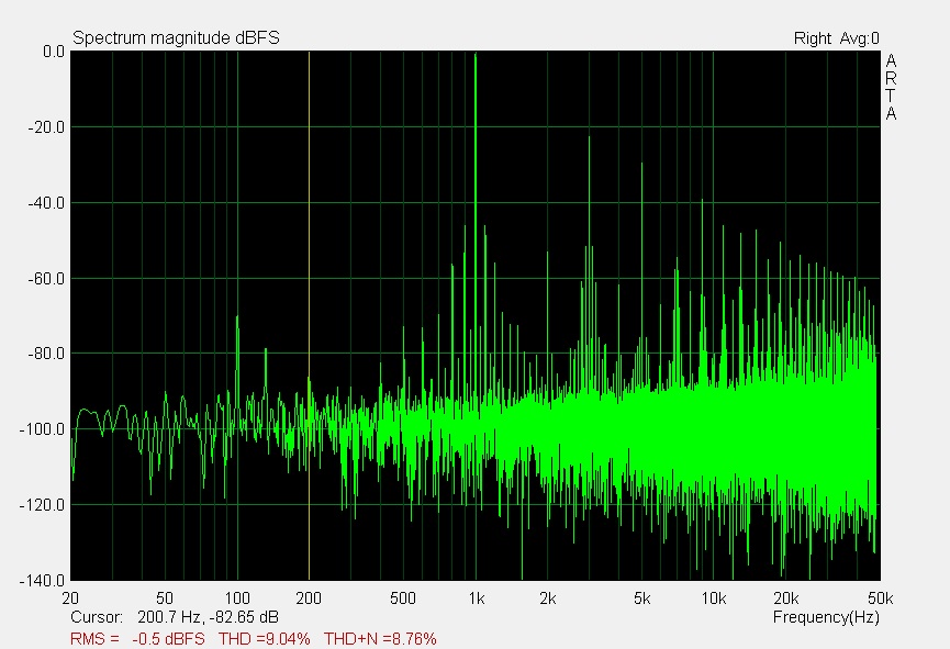
And now 9% THD.
The 0.35% you could perhaps live with, but the 9% looks utterly horrible. No one would ever want to listen to anything with that going on, at least not if they didn't want to get a headache. Quite why TI quote the power level at 10% THD I don't know as it isn't really representative of any real world situation. Most people would turn it down if it got to that point.
That's basically it as far as my measurements went.
In conclusion I can say that the Ice Components inductors didn't appear to break a sweat in the least. The overall performance being roughly what TI state for the PBTL mode as being around 0.05%. The increase in distortion towards high frequencies doesn't appear to be related to the inductors, otherwise I'd expect to see worse performance at higher output currents. With that in mind I think IceC have done a great job with their new product line. It would be nice to do some tests with a switch mode PSU where, regardless of current draw, the voltage would remain fixed at 50 volts. But until that point I don't have anything bad to say.
With regards to the amplifiers overall performance. They obviously don't come close to beating a well designed class A or B amplifier in the distortion stakes. However when it comes to efficiency, size and power output, they really can't be rivalled (unless by another digital amp
) With an appropriately spec'd PSU you should be able to get 100/200/400 watts into 8/4/2 ohms whilst keeping the distortion acceptably low. For most listening levels the distortion should also be in the noise floor.
I'm currently using my pair to drive the bass section of my loudspeakers, which are dipole. The efficiency here, I welcome without a doubt, and on top of that they sound great.
With regards to subjective comments run full range, I don't have any, at least not yet, and not with the new inductors. When I get around to hooking them up to a passive pair of speakers I might decide to comment on that. But for the time being I've got other matters to attend to.
From my point of view, I think I'd choose a well designed solid state amp for critical listening and use the digital ones where you can get the most from them and IMO that's Either in HT or in higher powered applications, where you'll be glad for the efficiency.
Under normal listening levels I don't use more then, around 1-5 watts to the individual drivers. So at least for my application having the other 6 channels classD wouldn't really be worth it.
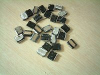
I can't understand ,do you realy get your data in your test ,when you adjust voltage to 50V,and output 2*200w/4ohm,and use your PCb,you will get burning.this chip refuse any over voltage pulse,Sound good ,Use carefully.
Pcb routing very importent.I have to burn one or two chip when I get it one really data,there are 50-100 burned chip in my waste tank.lots of money had married to TAS series,I have tested TAS5615 also,So trouble,don't use it at 50V,low voltage like 35v enough.works stablity.TAS series have excellent sound ,I think due to BB company merged by TI.good op amp and other special circuit inside.upload some of burned chip pic , so expensive.thus called "DIY".
Pcb routing very importent.I have to burn one or two chip when I get it one really data,there are 50-100 burned chip in my waste tank.lots of money had married to TAS series,I have tested TAS5615 also,So trouble,don't use it at 50V,low voltage like 35v enough.works stablity.TAS series have excellent sound ,I think due to BB company merged by TI.good op amp and other special circuit inside.upload some of burned chip pic , so expensive.thus called "DIY".
Attachments
Last edited:
I can't understand ,do you realy get your data in your test ,when you adjust voltage to 50V,and output 2*200w/4ohm,and use your PCb,you will get burning.this chip refuse any over voltage pulse,Sound good ,Use carefully.
Pcb routing very importent.I have to burn one or two chip when I get it one really data,there are 50-100 burned chip in my waste tank.lots of money had married to TAS series,I have tested TAS5615 also,So trouble,don't use it at 50V,low voltage like 35v enough.works stablity.TAS series have excellent sound ,I think due to BB company merged by TI.good op amp and other special circuit inside.upload some of burned chip pic , so expensive.thus called "DIY".
Gosh that's a lot of dead chips
I have wondered if they can really put out the claimed 600 watts in PBTL mode. And I've always been worried about blowing something up when testing.
I too have destroyed 4 of them I think up to now, but that was from miss use.
A responsibility designer must know well you design product works good or bad at worst use condition,Never believe the data from lab until you try it yourself.when you finish it .you'll get stable product.discrete component circuit is easy analyze,IC not easy,block diagram not tell us details.you must try it many a time.
Do you think the horrible distortion is the amp clipping or a horrible built in limiter? I thought class D amps should never be allowed to clip, and I think your pictures show why.
Anybody got a nice circuit for a fast, hard limiter that doesn't sound too horrible? Or an accurate just-about-to-clip indicator?
Anybody got a nice circuit for a fast, hard limiter that doesn't sound too horrible? Or an accurate just-about-to-clip indicator?
- Status
- This old topic is closed. If you want to reopen this topic, contact a moderator using the "Report Post" button.