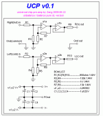
there are lots of wonderful opamp manufactured by nsc,ad and ti.i plan to make a universal pre-amp basis on the chips.
design goal:
1,simple configuration,
the unit will use 2pcs universal dual opamp.
2,pure dc coupling,
the unit will not include caps in the signal route.no high(low)-pass filtering,dc block.maybe setup some break points for unstable op.
3,diy friendly,
make the pcb compact,easy install,easy embed.
-zang
DC coupled pre-amp
DC coupling requires DC detection and some form of input and/or output muting if the detection activates.
Consider adding a DC servo to minimise the "normal" offset.
Ensure you have adequate RF filtering.
I have now done some smd assembly using To23 and 805 resistors/caps. Don't be afraid to use these sizes. It was relatively easy for my magnifying glass assisted old eyes.
Ted205 said:why have you used an output buffer ?
the buffer stage was setup for connection friendly,it can fix impedance problem of the after device such as connection cable,volume pot,power amp...
Atilla said:If you want to add a dedicated buffer after the opamp, you might want to consider to put it inside the feedback loop of the opamp. Look at the LME49600 application notes for example, I find it to be more beneficial.
this is a design case.the u1a,u2a voltage gain is isolated with the u1b,u2b buffer.
i have tested the overall loop configuration.it work good but it is no good for pre-amp.
if i make a headphone amp i will use overall loop.
Digi,
You might want to look at the Pimeta and PPA amps on tangentsoft.net, and then remove the dedicated ground channel. They're both basically the same thing -- OPamp gainstage followed by a buffer. Tangent/Phil have a lot of good info on the site regarding the headphone amps built with the nested feedback loops (I think it's mostly from Walt Jung).
That said, I think it would be nice to have the following:
1) Onboard power regulators with the option to use both dual secondaries (like a gainclone) or a center tapped (by leaving some diodes out). Maybe even something so you could have two "dual mono" preamps on the same board? LM317/337s would be fine, but discrete regulators would be nice if.
2) Spots for different sized potentiometers.. Alps RK27 and RK097?
3) Pads for SMD and DIP chips (this is pretty easy).
Motherone, I was thinking of using Tangent's setup for a preamp, that's why I raised the question above. digi01 seems to have a reason to follow that design though. While a more detailed explanation (I'm fairly noobish so forgive me, please) would help, digi01, an experiment would be of the biggest benefit, at any rate.
to lgreen,motherone,
cause this is a pre-amp design,it is very different from headphone amp.
for a pre-amp,the before connections will be kinds of source(cd player,pc auduio interface,mp3,ipod),the voltage level is around 0.7V to 2V.the after connections will be kinds of resistance load(cables,pots).i assume the pre-amp will driver a long cable end with one fix resistor.
the headphone amp is inductance load,it is more complicated than pre-amp.the Pimeta and PPA amps is headphone amp,i admire they designer i hope i can design headamp after some days.
so,i think the most important thing of pre-amp is impedance matching,the second important thing is drive ability.that is why we use pre-amp in audio gear.950ohm link is a better value for pre-amp.sure 100ohm will works.
i agreed onboard,it is diy friendly") but i do not like onboard psu for gain stage device.there are so many noise issue,trust me.you can check brand audio,factory evaluation board.no one use it.the gain stage at least far away from psu 120mm.
but i do not like onboard psu for gain stage device.there are so many noise issue,trust me.you can check brand audio,factory evaluation board.no one use it.the gain stage at least far away from psu 120mm.
pots on the board is a good way to reduction signal route.i will consider it.but this is pre-amp balanced & unbalanced design.on board pot will no use for the balance setting.
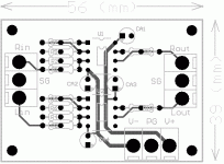
smd&pdip combine footprint is good.the below is a test layout.
to sawreyrw,
yeah,i am working on it.
Zang
cause this is a pre-amp design,it is very different from headphone amp.
for a pre-amp,the before connections will be kinds of source(cd player,pc auduio interface,mp3,ipod),the voltage level is around 0.7V to 2V.the after connections will be kinds of resistance load(cables,pots).i assume the pre-amp will driver a long cable end with one fix resistor.
the headphone amp is inductance load,it is more complicated than pre-amp.the Pimeta and PPA amps is headphone amp,i admire they designer i hope i can design headamp after some days.
so,i think the most important thing of pre-amp is impedance matching,the second important thing is drive ability.that is why we use pre-amp in audio gear.950ohm link is a better value for pre-amp.sure 100ohm will works.
i agreed onboard,it is diy friendly
but i do not like onboard psu for gain stage device.there are so many noise issue,trust me.you can check brand audio,factory evaluation board.no one use it.the gain stage at least far away from psu 120mm.pots on the board is a good way to reduction signal route.i will consider it.but this is pre-amp balanced & unbalanced design.on board pot will no use for the balance setting.
smd&pdip combine footprint is good.the below is a test layout.
to sawreyrw,
yeah,i am working on it.
Zang
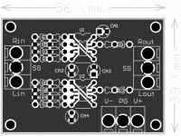
Attachments
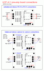
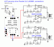
the below pic is the board connections,its show standard stereo and balanced setting.in balanced mode,the chip u1 for active,u2 for passive.
this pre-amp is volume pot free design.if needed can add 10k volume pot before the input or after the output.
this pre-amp is volume pot free design.if needed can add 10k volume pot before the input or after the output.
Attachments
That should do it, more or less. You can afford to use a higher-value pot - 50k, maybe even 100k without any problems and you'll get even higher input impedance.
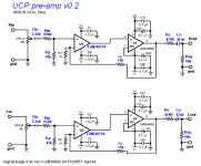
I'll get around to try to make a layout for what I'm planning one of those days as well. My first try to make a board layout
I'll get around to try to make a layout for what I'm planning one of those days as well. My first try to make a board layout
digi01 said:Atilla,
i made it! this ucp v2 is a after design of the nsc's classic application.i modify it for pre-amp bettter.
i just have few samplers in stock,i hope i can find some time to test this configuration.
zang
sounds interesting.. would you be able to provide pcbs?
tent:wq
- Status
- This old topic is closed. If you want to reopen this topic, contact a moderator using the "Report Post" button.
- Home
- Amplifiers
- Chip Amps
- universal chip pre-amp project