I am playing around with the design for my aikido line stage that I want to integrate a phono stage into. I have been weighing between some type of board stuffed guts or point to point for the phono section and still can not decide.
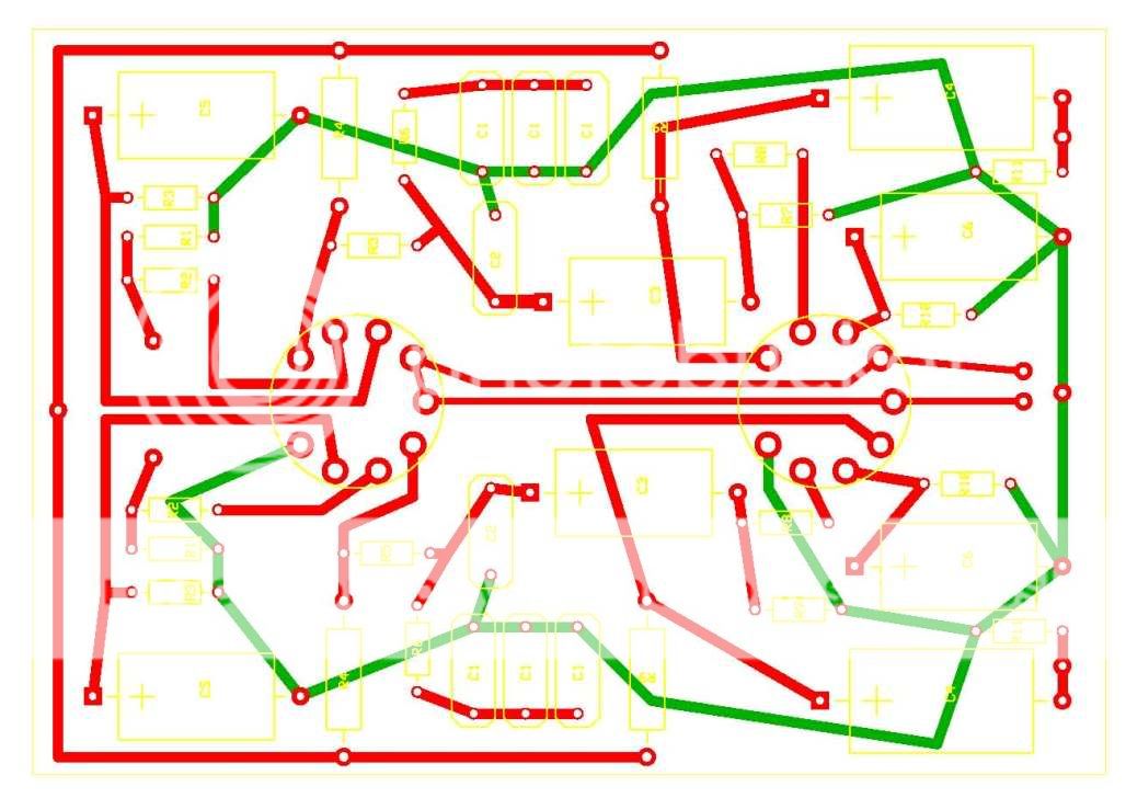
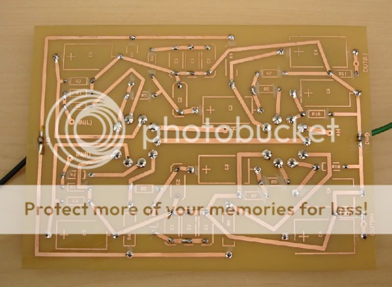
I drew up this little PCB section today...I would do the old copper board - toner transfer technique with this.
Does this board layout look OK? I have never laid out a board before...
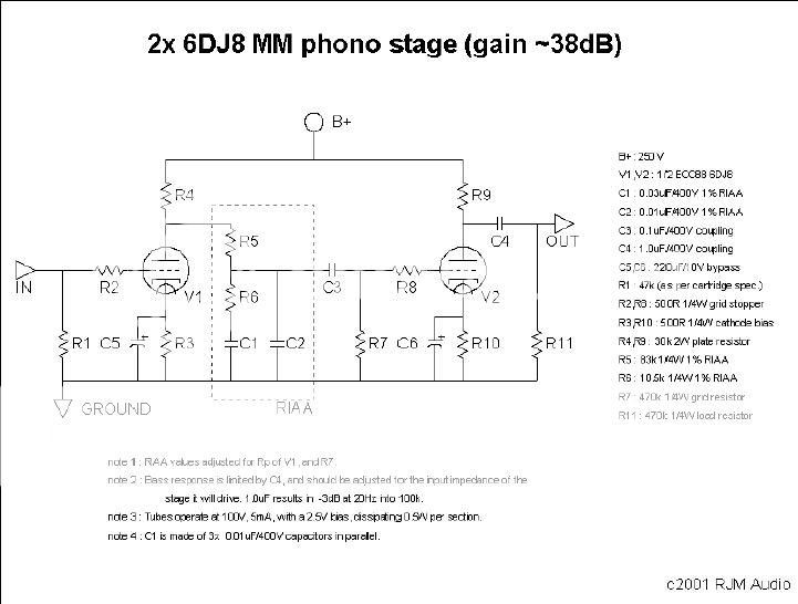
The schematic is the RJM 6DJ8 phono stage - with the suggestion of having the tubes run in series instead of parallel - I.E...each tube has a L and R channel instead of a dedicated L tube and R tube...
I drew up this little PCB section today...I would do the old copper board - toner transfer technique with this.
Does this board layout look OK? I have never laid out a board before...
The schematic is the RJM 6DJ8 phono stage - with the suggestion of having the tubes run in series instead of parallel - I.E...each tube has a L and R channel instead of a dedicated L tube and R tube...
HollowState said:My advice would be to post a smaller picture. This one stretches more then twice my monitor's width and is very annoying. It also streches the text with it. Whenever I see a post like this I click away and don't bother with it.
Point taken....
Ahhh...thanks for that catch!!! I figure I should post the schematic too - if that helps any...
An externally hosted image should be here but it was not working when we last tested it.
nigelwright7557 said:Thicker tracks where possible, always makes etching easier/better and helps save the planet too !
Why have you got red and green tracks, that usually means you have two layers ?
I visualized the red for hot and the green for ground. The board is all one layer. It made it easier to track the circuit...
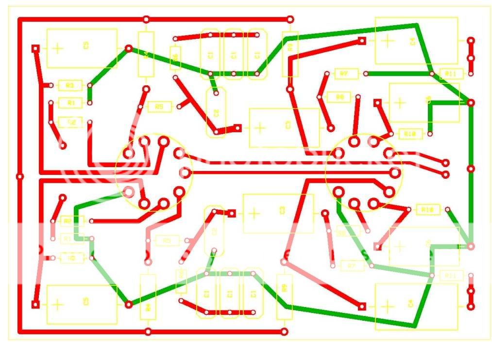
cjkpkg said:OK...Here is the latest. I realized that I also needed to run the filaments in series versus parallel...I think I did it right...
Hi Carl,
If I were going to layout a circuit board for this preamp, I would do it in such a way as to not run any traces through two adjacent tube pins. I would also limit it to only one trace going through the 1-9 pin space. Even if you have to use wire jumpers on the top surface to accomplish this. Cramming three lines through the 1-9 opening is not good layout practice in my opinion.
Also, the filament lines should be the widest of them all because they carry the most current. Your's are the thinner of the bunch. Signal lines could be thinner if necessary because they carry virtually no power, although I see no need for that with this simple circuit.
I'll admit that I have no experience with computer aided circuit board design because anything I did years ago was by paper and pencil. But the CAD programs of today should make things much easier. Perhaps give it another try.
Victor
Hi
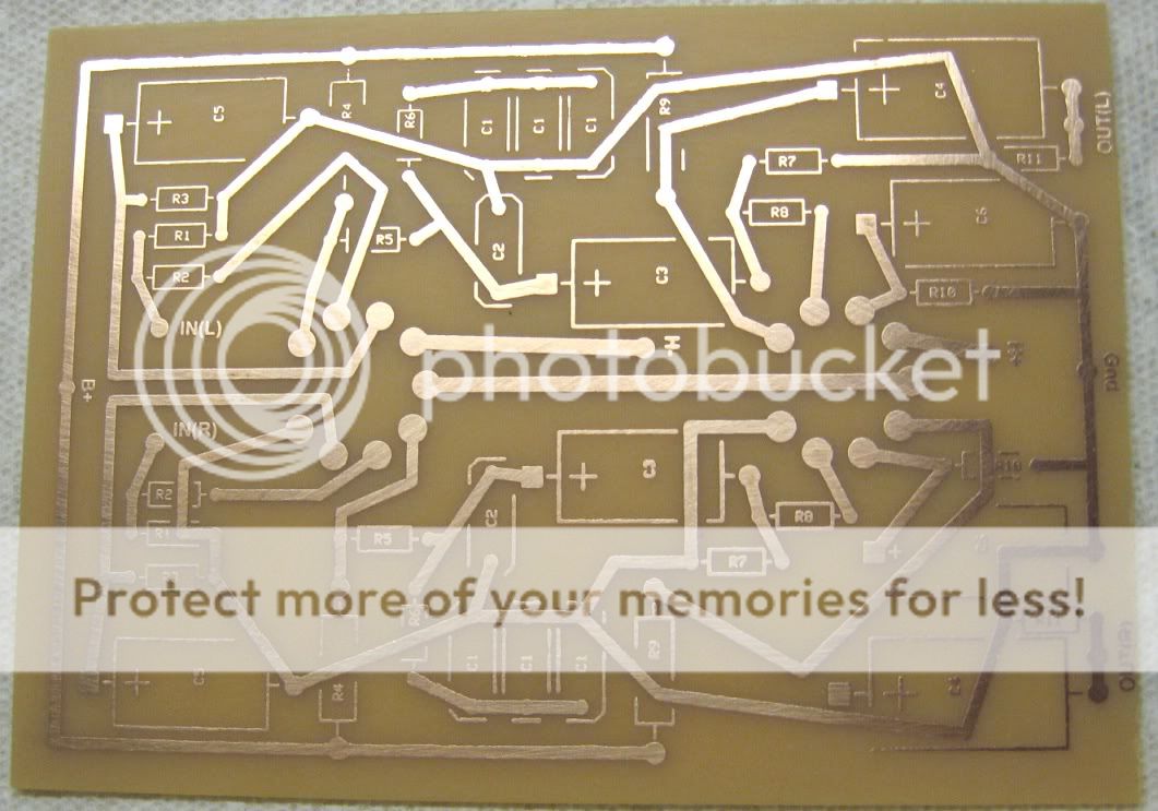
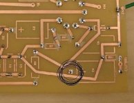
I would not include the component overlay on the copperside of a valve/tube PCB.
With some of the voltages running on a valve/tube PCB you may just get an arc-over and wham!!!
But then I am over cautious and a nit picker about things that things that may go wizz-zap-wham and you smell that acrid stink of an electronic part "stepping-over" beyond it's design limits!
Great looking etched PCB there by the way. What tools process do you use to produce PCB's?
I did the laser jet printout on a transparency. Iron it on and give it a Ferric Chloride bath...
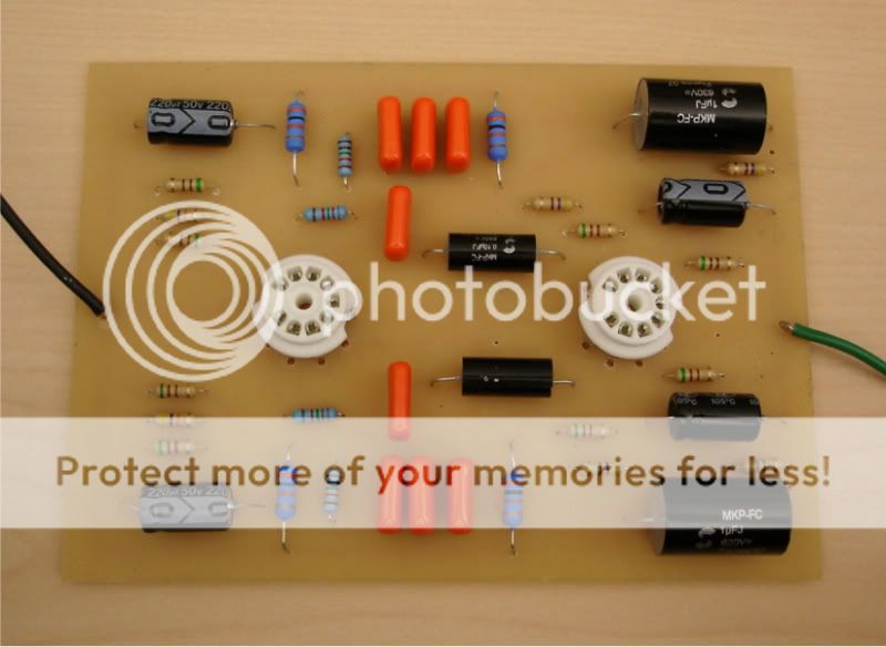
I do plan to coat the solder side after it is stuffed...I have seen some folks recommend using just a clearcoat acrylic. Would this be OK??? Or maybe a clear polyurethane?
Any advice here would be appreciated.
Carl
I do plan to coat the solder side after it is stuffed...I have seen some folks recommend using just a clearcoat acrylic. Would this be OK??? Or maybe a clear polyurethane?
Any advice here would be appreciated.
Carl
- Status
- This old topic is closed. If you want to reopen this topic, contact a moderator using the "Report Post" button.
- Home
- Amplifiers
- Tubes / Valves
- PCB advice