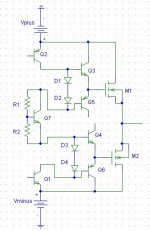
I saw this circuit in the datasheet of the PAD126, released by Power Amp Design (www.powerampdesign.net). I have reproduced a version of it in PSPICE to make this included picture. I was curious as to why each output transistor has both an NPN and a PNP driving its gate (for a total of four driver transistors instead of two).
Q2 is the common emitter, and Q1 is the current source/active load. There is a vbe multiplier (Q7), and the output transistors are M1 and M2.
For a cleaner schematic, I skipped two connections. Assume that the collector of Q5 is tied to the minus rail, and the collector of Q4 is tied to the plus rail.
I am assuming that the driver stage (between VAS and output stages) is composed of Q3, Q4, Q5, and Q6.
--> Why does each output transistor have both an NPN and a PNP driver? I have never seen this before with the "extra" transistors (the PNP Q5 for the N-type output transistor, and the NPN Q4 for the P-type output transistor).
Attachments
- Status
- Not open for further replies.