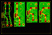
The attached image shows 4 variations of a small and simple PCB design for an adjustable LDO regulator such as the LT1084 or LT1085 and would be used to power the smaller Tripath chip amps like the SI, amp3, etc. Can anyone with PCB design experience tell me which layout would be best or how a layout could be improved? The first design only uses the bottom layer (in green). The other three designs use the top layer (red/orange color) for power traces and bottom layer as the ground plane.
I tried to make them as compact as possible not only to keep traces short but because I'd like to house this little fellow in a small chassis with the amplfier. This allows the transformer, rectifier, and filter caps to be situated in their own separate case. The dimensions of the design with the largest ground plane is only 1" by 2". The smaller ones are only 1" by 1.75". The pot allows the output voltage to be adjusted and the small cap right next to the pot is for 120Hz ripple rejection. The smaller bypass caps across the larger bulk caps could be small value ceramics or even MKP or MKT types if the lead spacing is right. No protection diode is necessary with the LT108X regulators for this type of operation so I chose not to include one.
Thanks for any help.
Attachments


- Status
- This old topic is closed. If you want to reopen this topic, contact a moderator using the "Report Post" button.