Let me start by saying, I've found all kinds of terrific information on this board- it is a great resource for SMPS design!
I am trying to work out the final kinks in my half-bridge 2000W audio amplifier power supply. Everything is working pretty good as far as regulation and ripple. I am using 2 punch-through Advanced Power IGBT's (thanks to Eva for the IGBT suggestions") ) The converter is running at 100kHz effective (200kHz clock) with a MC34025 controller (current mode). I am using a gate transformer wound on an EE19 core with 11TS primary and 11TS secondaries.
) The converter is running at 100kHz effective (200kHz clock) with a MC34025 controller (current mode). I am using a gate transformer wound on an EE19 core with 11TS primary and 11TS secondaries.
My main transformer is on an ETD49 core. Primary turns is 18TS wound between the 2 secondary halves of 10TS. (Split secondary construction) I'm using 0.1mm copper strip for adaqate current capacity and lower leakage (I think ) No PFC on this supply, 320 DC peak on the bulk DC caps. +/-68 VDC rails on the output. Output has coupled inductor with 320uH per output and 940uF capacitance per rail. I'm usng some great ST diodes (STTH8R06D) on the secondary in full bridge config.
My problem is my IGBT's are heating up quite rapidly because I had to slow thier on time switching speed rate a bit (w/ 47ohm gate R's). This is due to the fact the with very fast rise, the current spike and ringing as seen through the primary of the transformer was so great it was causing all kinds of RF noise on the amplifier and who knows what the EMI would look like on the spectrum analyser. As I increase the gate resistance, the ringing is almost gone and so is the noise on the amp. This, of course, creates unaccaptable heat on the IGBT's.
I've tried different transformer arrangements and can't seem to improve this at all. I think my layout is pretty tight with wide tracks in the power loop. (I'm not sure I have a way to post the PCB layout or the schem.) I keep thinking I'm doing something wrong with the way the transformer is wound and I'm getting excessive leakage inductance. I can't live with the heat, so do I try some sort of current snubber arrangement, and if so, where does it go? I currently don't have any additional inductors or caps in the primary path- should there be?
Thanks for any and all help- it's been frustrating me for some time
Matt.
I am trying to work out the final kinks in my half-bridge 2000W audio amplifier power supply. Everything is working pretty good as far as regulation and ripple. I am using 2 punch-through Advanced Power IGBT's (thanks to Eva for the IGBT suggestions
) The converter is running at 100kHz effective (200kHz clock) with a MC34025 controller (current mode). I am using a gate transformer wound on an EE19 core with 11TS primary and 11TS secondaries.My main transformer is on an ETD49 core. Primary turns is 18TS wound between the 2 secondary halves of 10TS. (Split secondary construction) I'm using 0.1mm copper strip for adaqate current capacity and lower leakage (I think
) No PFC on this supply, 320 DC peak on the bulk DC caps. +/-68 VDC rails on the output. Output has coupled inductor with 320uH per output and 940uF capacitance per rail. I'm usng some great ST diodes (STTH8R06D) on the secondary in full bridge config. My problem is my IGBT's are heating up quite rapidly because I had to slow thier on time switching speed rate a bit (w/ 47ohm gate R's). This is due to the fact the with very fast rise, the current spike and ringing as seen through the primary of the transformer was so great it was causing all kinds of RF noise on the amplifier and who knows what the EMI would look like on the spectrum analyser. As I increase the gate resistance, the ringing is almost gone and so is the noise on the amp. This, of course, creates unaccaptable heat on the IGBT's.
I've tried different transformer arrangements and can't seem to improve this at all. I think my layout is pretty tight with wide tracks in the power loop. (I'm not sure I have a way to post the PCB layout or the schem.) I keep thinking I'm doing something wrong with the way the transformer is wound and I'm getting excessive leakage inductance. I can't live with the heat, so do I try some sort of current snubber arrangement, and if so, where does it go? I currently don't have any additional inductors or caps in the primary path- should there be?
Thanks for any and all help- it's been frustrating me for some time
Matt.
Eva,
Yes- with mylar sandwiched in between. It was my understanding that this would lead to lowest leakage inductace. I tried wire wound transformers, but saw no difference in performance that I could tell. Perhaps I should go back to the transformer design stage
I also see the same ringing as a voltage ring on the output diodes. Snubbing them only helps a little.
Are you aware that 18 turns of copper foil with the width allowed by an ETD49 coil former are going to produce a huge winding capacitance?
Also, leakage inductance is not such a bad thing, it has some great properties like smoothing reverse recovery from secondary winding diodes and allowing the switches to saturate before the current has reached its maximum value, thus reducing dissipation.
Also, leakage inductance is not such a bad thing, it has some great properties like smoothing reverse recovery from secondary winding diodes and allowing the switches to saturate before the current has reached its maximum value, thus reducing dissipation.
I tried winding another xfmr with triple insulated wire. S=SH=P=SH=S (SH means 'shield'), one layer each for each half of the secondary and the primary. I also added a shield layer in between each half of the secondary and the primary. I see no difference The shields help a bit, but not as much as I hoped.
Back to the drawing board...
I may try winding it more conventionally as split-primary P=SH=S=S=SH=P and see if I have better results.
The shields help a bit, but not as much as I hoped.Back to the drawing board...
I may try winding it more conventionally as split-primary P=SH=S=S=SH=P and see if I have better results.
I have not been able to find a way to get a picture of it yet, and my layout/schem is done on a Mac, of all things, so I need to find a way to transfer to JPEG. I do have a way to post waveforms- I will try to post the current waveform with gate drive and Vce waveforem for one IGBT.
I'm going to stick with wire windings since there is no improvement with foil. I suppose foil would be useful for high current, low voltage secondary windings. I had just noticed that a QSC amp had a transformer with all foil windings and thought I'd give it a try. Wire is WAY easier to work with anyways and that makes things much easier.
I'm going to stick with wire windings since there is no improvement with foil. I suppose foil would be useful for high current, low voltage secondary windings. I had just noticed that a QSC amp had a transformer with all foil windings and thought I'd give it a try. Wire is WAY easier to work with anyways and that makes things much easier.
Thanks to a nice scope borrowed from work, I'm able to show these waveforms. This is with barely any load. (Amplifier at idle.)
The light blue is the current through the primary of the transformer.
The dark blue is the Vce of one of the IGBT's
The green is the gate voltage of the same IGBT.
The light blue is the current through the primary of the transformer.
The dark blue is the Vce of one of the IGBT's
The green is the gate voltage of the same IGBT.
Attachments
I would guess that you need a smoother gate drive. Still fast rising for efficiency, but rounded off a bit to cut down on transformer ringing. High power SMPS FET stuff I see at work tends to use low source impedance transformer drive feeding the gates through a 10R in parallel with a small fast forward diode, with a capacitor from gate to source or the earthy end of the drive winding depending if there's a source current sense. The capacitor is usually somewhere in the 1nF to 10nF region and is tuned to as low a value as necessary to stop ringing. I haven't used IGBT's so whether this is any use, dunno.
You are turning on the IGBTs far too fast, and your transformers and/or layout also suffer from an awkward resonance characteristic and a lot of capacitance. An approach to get slow turn-on but fast turn-off is to use a big value gate resistor and place in paralell with it a small value resistor with diode in series for fast turn-off. Where are you measuring the current? If that trace is actually transformer current, then you may be suffering from a severe reverse recovery issue in the output diodes.
Also, I'm wondering why the gate of each set of IGBTs doesn't get negative drive when the other ser of IGBTs are turned on. Do you have additional buffers between the gate drive transformers and the gates?
Also, I'm wondering why the gate of each set of IGBTs doesn't get negative drive when the other ser of IGBTs are turned on. Do you have additional buffers between the gate drive transformers and the gates?
Thanks for your replies.
sbrads,
I have tried experimenting with the sort of thing you talk about, except I'm using an RC in series from gate to source. I will continue to give a look and see if I can improve the gate waveform with different values. I have not had much luck with this method yet.
Eva,
I have about 7ohms in series with each gate now. I'm trying for maximum efficiency, and when I start to increase that resistor, the IGBT's heat up more quickly. I guess I need to find the point where the ringing isn't too bad and the heat is acceptable. As you suspect, I do have an additional PNP/diode turn off circuit in series with gate drive, so there will be no negative bias in the off state- gate is shorted to source when drive pulse is negative. I did this to take some burden off of the controller IC drive current. Also, turn off current is localized to the IGBT this way. I saw this in a Unitrode seminar, and it seemed like a good idea.
BTW, the blue trace is measuring xfmr current. I agree that it is probably a capacitance/resonance problem somewhere. I am using some really fast diodes that should be well suited for this application- STTH8R06D. I originally had MUR860 in there, but the voltage spikes were at lease twice as large.
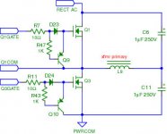
This is simple and effective, but it has a major flaw: The CB junctions of Q9 and Q10 are being reverse biased during the negative going pulse, and I think that this is causing parasitistic turn-on of the transistors and that strange and abrupt gate turn-on characteristic.
I usually do it in another way and it works fine. To do it that way, replace R43 and R47 by jumpers, then insert additional diodes in series with the 10 ohm turn-on resistors, and finally place the 1K base turn-off resistors between the bases of Q9 and Q10 and ground (source) instead. This produces some kind of automatic "turn-off", altough the benefits of driving the 1K resistor from a negative voltage are lost. A small RC snubber may be required to damp potential gate transformer ringing. Alternatively, R43 and R47 may be split in two 470 ohm halves, and a clamping diode may be inserted between the middle points and ground to prevent reverse biasing.
I usually do it in another way and it works fine. To do it that way, replace R43 and R47 by jumpers, then insert additional diodes in series with the 10 ohm turn-on resistors, and finally place the 1K base turn-off resistors between the bases of Q9 and Q10 and ground (source) instead. This produces some kind of automatic "turn-off", altough the benefits of driving the 1K resistor from a negative voltage are lost. A small RC snubber may be required to damp potential gate transformer ringing. Alternatively, R43 and R47 may be split in two 470 ohm halves, and a clamping diode may be inserted between the middle points and ground to prevent reverse biasing.
Eva said:You are turning on the IGBTs far too fast,
I don't agree .....2kW poke at 100Khz operation is pushing ones luck with IGBT's......all the notes I've come across recommend derating the operating frequency i.e 50Khz at this power level or less. I thought it was the slow turn-off tail current at that frequency that is a major contributor of device heating.
As you have already made a core....one is stuck without a redesign to larger core.
An ETD49 core at 100Khz running at 2kW will certainly get hot and the circuit won't like transients. Did you select core size based on Joules = I squared L ?
richj
I don't recall if you've monitored this yet, but you want to make absolutely sure there is no cross conduction between the upper and lower IGBTs. This will cause them to heat up in a big hurry. You should be able to find out really quickly by hanging a DC current probe on either IGBT - you won't be able to see cross conduction by monitoring the transformer current.
I would like to see the rest of the driver circuit, as I am curious about how you are level shifting the drive to the upper IGBT. Ideally, you want slow turn on and fast turn off to avoid cross conduction. I use the PNP turn off boost trick quite a bit myself, but I usually put a resistor to ground (source) from the PNP base rather than the arrangement you showed. Depending on the PNP gain, 1K might be a little too large to adequately drive the transistor - remember, it will probably need to be conducting an amp or two of peak current in order to turn off the IGBT quickly. It is also a good idea to hang a resistor directly from gate to source on each IGBT in order to have some assured turn off impedance at each gate.
If you have both devices on the same heat sink, there also could be a possibility of the drain signal from one IGBT turning on the other. I've seen it happen with MOSFETs. If you have both devices on a common heat sink, You might want to pry one off briefly (use a separate heat sink if necessary) for diagnostic purposes. Another dodge might be to temporarily use double or triple silpads on one device to reduce the capacitance to the heat sink. Grounding the heat sink to primary return will also help to reduce cross-talk between devices on a common heat sink.
Remember also that the intrinsic diodes on each IGBT will conduct to carry the XFMR magnetizing current during the switch dead time. When you turn on a switch again, it will force recovery of the intrinsic diode - if the magnetizing current is large, this may cause a reverse recovery zatch. You can easily calculate the mag current from the primary inductance of the transformer, applied voltage, and duty cycle. You can also see it directly by monitoring the transformer current. I''m a bit concerned that the mag current could be fairly high, as the number of primary turns used is relatively small. However, this is not my biggest concen for the design, as there are some questions about the drive that should be sorted out first. As a last-ditch diagnostic measure, you can try putting a schottky diode in series with each switch, with an ultrafast diode around the combination of schottky and IGBT. This will keep the magnetizing current out of the IGBT intrinsic diode during the switch dead time, so that you can determine if it is causing a problem. I've actually seen this technique used as a matter of course on some high power half-bridge power supplies (quite possibly resonant supplies, as they were used for high-power, high voltage applications). This was pretty important with earlier generation MOSFETs that did not like to have their intrinsic diodes jerked abruptly into recovery. This technique is probably more important for a resonant half bridge than a conventional design, as the magnetizing current on a conventional half bridge will be relatively small if the transformer is designed properly. However, if a series resonant half bridge supply drops below resonance, you can get substantial commutation current during the switch dead time.
Thanks for all the replies so far.
wrenchone: I'm using a 1:1 transformer for level shifting, with each end of the primary connected to OUTA and OUTB of the driver.
rich walters: These IGBT's are made to replace MOSFETS and are rated for 22A current @ 100kHz. The technology is "punch-through" as aopposed to "non-punch through". They have finally found a way to pretty much eliminate the long tail turn-off. (I forget the process, but they add another doping layer, or something) Check out advancedpower.com for more info.
Eva: I'll play around with the turn-off method and see if I get an improvement.
I will ponder the suggestions and post as soon as I have a chance to try a few more things out.
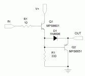
Hmmm... I would think that you only want to use the level shift transformer on one of the outputs. If you have it driving both outputs, the stored magnetizing energy from one 1/2 cycle will try to turn the opposite driver on during the output driver dead time. Let me know if I've misinterpereted what you're doing, but that's my take on it. I'd use the transformer to drive the top IGBT, and maybe buffer the output that drives the bottom device (or both outputs). Attached is a suggested buffer circuit.
Attachments
More experimentation and I've found that my coupled inductor needs improvement. I currently have it wound bifilar and connect the opposite leads to flip phase on one output. I was just going over a Lloyd Dixon note on coupled inductors and he suggests the windings should start together and be wound in opposite directions on the core so the noisy end of one winding doesn't couple capacitively to the clean end of the other winding. In other words, the winding ends that connect to the diodes should start together and be wound in opposite directions around the core. I have them wound the same direction and just connect it such that one is out of phase.
It's kind of hard to explain.
I put separate inductors on each output and my spike was the same amplitude, much higher frequency, but shorter duration ringing. I think this is an improvement.
I will try to rewind the output inductor differently.
I also experimented with different gate drive arrangements and may stick with the classic R in parallel with the diode and skip the PNP turn off deal. The diode I am using in that arrangment seemed to slow the turn on down. It is a 4148, which I would think is fast enough, but turn on time suffered. Also, as wrenchone suggested, the 1K drive was not adequate enough to turn off the PNP. I may go back and try it again later, as it definitely eases the job of the controller, but will drop it for now.
- Status
- This old topic is closed. If you want to reopen this topic, contact a moderator using the "Report Post" button.
- Home
- Amplifiers
- Power Supplies
- Current ringing in SMPS