These waveforms look right to me. In order for gate ringing to happen you need excessive inductance in the gate drive wiring, I would try to improve that if I was you.
How did you manage to blow that little IGBT?
In such a slow-switching circuit you could even use medium speed IGBTs, those that feature only 1V or so voltage drop and 100 to 200ns smooth rise times, or even bipolar transistors xD
I've been doing a lot of work in the 15V 120A prototype, I will post details soon to let you see how much performance could be obtained from four bipolar transistors worth not more than 5 euro in total.
I don't think that this set up has high inductances in the gate drive.
...well, at least there is no space left open. The loop area is about
80mm^2, mainly shaped like 2x40mm side aside. (Base from the most far away PNP ==> emitter resitors ==> both gates ==> both sources ==> source resistors ==> GND foil backwards to the collector of the PNPs==> base).
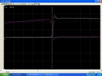
The ringing was one or two times "pull up slash back", at the moment when the drain jumps upwards. Feedback through reverse capacitance of the MosFets.... Gate drive resistance seemed to be the only key to improve this.
I tried to simulate this, as from theory already the reverse capacity with the intrinsic MosFet gate source capacity and inside inductance could cause ringing. During turn OFF the MosFet is acting like a normal
amplifier with cap. feedback and inductive load...
Well the simulation did not show any ringing. Even not with additional
inductors in the gate grive. Theory vs. reality...")
The IGBT simply died, without obvious reason.
But quite spectacular...
The wave forms looked not perfect, but acceptable at that moment.
Peak current was around 6A....
I just wanted to measure the temperature with my infrared themometer, ...touch free measurement... - ZONK !!!!
....some seconds later, after my heart started beating again, I went on to measure the temperatures of the carbonized resistors and found them at 58°C (burned & open)... the IGBT around 50°C (blown: C-E shortened, gate open)....
Do you think there might have been some critical reverse load for the IGBT? I did not place an external diode between C & E.
...or voltage overshoot above 600V...( did not look to this value very detailed)...
Looking forward to your 15V/120A PSU.
...well, at least there is no space left open. The loop area is about
80mm^2, mainly shaped like 2x40mm side aside. (Base from the most far away PNP ==> emitter resitors ==> both gates ==> both sources ==> source resistors ==> GND foil backwards to the collector of the PNPs==> base).
The ringing was one or two times "pull up slash back", at the moment when the drain jumps upwards. Feedback through reverse capacitance of the MosFets.... Gate drive resistance seemed to be the only key to improve this.
I tried to simulate this, as from theory already the reverse capacity with the intrinsic MosFet gate source capacity and inside inductance could cause ringing. During turn OFF the MosFet is acting like a normal
amplifier with cap. feedback and inductive load...
Well the simulation did not show any ringing. Even not with additional
inductors in the gate grive. Theory vs. reality...
The IGBT simply died, without obvious reason.
But quite spectacular...
The wave forms looked not perfect, but acceptable at that moment.
Peak current was around 6A....
I just wanted to measure the temperature with my infrared themometer, ...touch free measurement... - ZONK !!!!
....some seconds later, after my heart started beating again, I went on to measure the temperatures of the carbonized resistors and found them at 58°C (burned & open)... the IGBT around 50°C (blown: C-E shortened, gate open)....
Do you think there might have been some critical reverse load for the IGBT? I did not place an external diode between C & E.
...or voltage overshoot above 600V...( did not look to this value very detailed)...
Looking forward to your 15V/120A PSU.
...picked up the topic again.
Even if the inductances were already small, this circuit has to handle quite high di/dt. Something like 700A/us !
I derived a further reduced inductance of the gate drive loop by paralleling another GND foil on the second side of the driver transistors.
Now the MOSFETS can turn of currents above 20A within less than 30ns without bad ringing.
Furtheron I corrected an error in the schematic: Feedback from output was drawn wrong, while I assembled my proto correctly....
Last but not least I optimized the regulation and reduced the output voltage down to 450V.
450V has the advantage that each e-cap can handle the full rail.
I prefer this, because I want to run a halfbridge converter from that and connect the cold end of the transformer to the center tap of the caps. If something goes wrong the center tap might be pulled to one of the rails and the e-caps will see full output voltage, not just half.
The optimisation of the regulation loop is a multiparameter optimization for wide input range, load range from zero to 1kW and audiable noise (you hear it, if it is not running perfectly smooth).
Attachments
I had to accept a trade off in THD and output regulation.
But overall performance is now satisfying my needs.
Input Voltage 120V/50Hz ==> output volatge:
No load: 435V
130W: 425V
335W: 409V
500W: 400V
700W: 356V
Input Voltage 230V/50Hz ==> output volatge:
No load: 447V
130W: 434V
360W: 429V
550W: 426V
900W: 420V
1070W: 418V
Input Voltage 270V/50Hz ==> output volatge:
No load: 447V (limited by overvoltage protection)
130W: 434V
360W: 431V
550W: 429V
900W: 423V
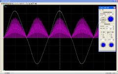
Current wave shape is quite nice at 120V.
Input: 120V/50Hz
Output: 500W
White trace: Line current 2A/Grid
Red trace: PFC choke current 6A/Grid
But overall performance is now satisfying my needs.
Input Voltage 120V/50Hz ==> output volatge:
No load: 435V
130W: 425V
335W: 409V
500W: 400V
700W: 356V
Input Voltage 230V/50Hz ==> output volatge:
No load: 447V
130W: 434V
360W: 429V
550W: 426V
900W: 420V
1070W: 418V
Input Voltage 270V/50Hz ==> output volatge:
No load: 447V (limited by overvoltage protection)
130W: 434V
360W: 431V
550W: 429V
900W: 423V
Current wave shape is quite nice at 120V.
Input: 120V/50Hz
Output: 500W
White trace: Line current 2A/Grid
Red trace: PFC choke current 6A/Grid
Attachments
Jaka Racman said:Hi,
I also agree with Eva about IGBT. I once designed two transistor (asymmetrical half bridge) laboratory flyback capacitor charger working in discontinious mode. I used large IR mosfet modules, but they failed regularly, until I exchanged them for first generation of IGBTs in TO247 case. Peak current was 70A and charger is still working today.
I am considering something similar for a booster/controller for my electric bicycle project. I had come up with the term quasi half bridge to describe it. I am glad you brought it up as well as ChocoHolic presenting this thread. Take care.
Hi Chocoholic. Congratulations, that's a nice job. However, those average current waveforms are not looking too well. I will try to get some captures from my continuous mode L4981 based PFC so that you can compare.
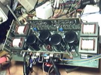
BTW: The 120V 20A AC class D amplifier is almost finished, this is how my prototype looks like:
BTW: The 120V 20A AC class D amplifier is almost finished, this is how my prototype looks like:
Attachments
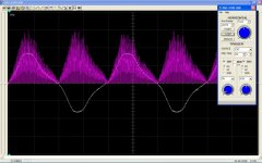
....looking not to well...
Hm, at 500W/120 it is looking almost perfect.
The difficulty was the trade off between wide input voltage range (which is influencing the gain of the forward transfer function).... extreme load range between zero and 1kW and my ears, which can hear the PFC working and are very sensitive to regulation modulations or even worse interuptions.
Originally I adjusted the regulation loop to get a nice sine wave also at 230V, but for this I had almost no P portion in the feedback loop and real integral (instead of two staggered PT1 ) .... resulting in quite poor regulation of load changes and interuptive operation at high input voltages at low load....
Also then I was not able to provide the 700W at 120V anymore. Now the P-portion of the regulator is pushing the current wave shape from sinusodial towards trapezoid shape in order to draw more current from the line, if the output starts to drop in a unpleasant way.
How did you solve all this without trade off in the THD? I thought these relations would be a fundamental drawback of this topology. Instability at low load is mostly caused by the two integrators. First integrator is the output cap with current feed and second is usually the integratot of the regulation loop.
And if you do something else than a slow integrator in the regulation, then you will not have sinusodial line currents anymore, because the regulator might act within each half wave.
Things are getting easier, if we move to large output caps.
As soon as remarkable changes of the output voltage are slow compared to the line period, we could use a slow PT1 regulator without violating the sinewave.
But who wants to use several thousand uF/450V....
??? ????
????
You solved it? ...you are starting to threaten me !!!
Hm, at 500W/120 it is looking almost perfect.
The difficulty was the trade off between wide input voltage range (which is influencing the gain of the forward transfer function).... extreme load range between zero and 1kW and my ears, which can hear the PFC working and are very sensitive to regulation modulations or even worse interuptions.
Originally I adjusted the regulation loop to get a nice sine wave also at 230V, but for this I had almost no P portion in the feedback loop and real integral (instead of two staggered PT1 ) .... resulting in quite poor regulation of load changes and interuptive operation at high input voltages at low load....
Also then I was not able to provide the 700W at 120V anymore. Now the P-portion of the regulator is pushing the current wave shape from sinusodial towards trapezoid shape in order to draw more current from the line, if the output starts to drop in a unpleasant way.
How did you solve all this without trade off in the THD? I thought these relations would be a fundamental drawback of this topology. Instability at low load is mostly caused by the two integrators. First integrator is the output cap with current feed and second is usually the integratot of the regulation loop.
And if you do something else than a slow integrator in the regulation, then you will not have sinusodial line currents anymore, because the regulator might act within each half wave.
Things are getting easier, if we move to large output caps.
As soon as remarkable changes of the output voltage are slow compared to the line period, we could use a slow PT1 regulator without violating the sinewave.
But who wants to use several thousand uF/450V....
???
????You solved it? ...you are starting to threaten me !!!
Eva said:
BTW: The 120V 20A AC class D amplifier is almost finished, this is how my prototype looks like:
This baby is looking somehow professional.
Nice lady, nice baby.

Hi Chocoholic,
I agree with Eva that your Haversine looks a bit strange. I would expect it to look more sinusiodal. The distortion looks rather large?
In my experience, load regulation is very poor when the PFC is working well. I let the OVP do it's work! Trying to compensate for reasonable load regulation upsets the modulation.
I haven't had any problems using FET's for 1kW power levels. Admittedly they're big ones. I've never worked with IGBT's.
Cheers, Ralph
Hi Ralph,
normally I would also say: OVP is fine.
But my ears could not bear the interuptive noise of the PFC in this mode. I really want use this stuff in my living room.
Fighting for 110db S/N ratio in the signal path, but allowing 40dbA noise floor in my listening room is not OK from my point of listening.
...well I could do some potting or varnishing of the PFC....
But, honestly... compared to normal current wave shapes caused by the traditional Transformer-Rectifier-eCap ...even this anti-noise-modified PFC is almost perfect. Isn't it?
You can improve load regulation and THD dramatically by employing a more sophisticated control IC with squarer and divider (like L4981A), since a much higher (and compensated) loop gain is allowed across the entire input voltage range that way.
L6560 is intended for low power low-cost applications.
L6560 is intended for low power low-cost applications.
Hi Choc,
I take your point about audible noise. My PFC was used in a non-audio application and the noise level was swamped by the cooling fan.
I also use the L4981 (B) and get very clean performance. It's a great part. The only issue with it is the low side current sense that makes system design a bit more tricky.
Sub 50kHz switching speeds, as Eva has mentioned, make EMC compliance much easier. The 3rd harmonic then lies below the start of the EMC limits (150kHz).
Cheers, Ralph
L4981....
Hm, I will definitely have a more detailed look to this.
Especially a simple possibility to implement a non linear (but smooth) regulation loop is looking quite promising to me.
May be my next PFC will make use of this IC. Good point.
...will dig at the part stores in Guangzhou and HongKong for this component and add to my assortment...
ChocoHolic said:L4981....
Maybe my next PFC will make use of this IC. Good point.
Check IR´s IR1150 also... doesnt get any easier than that.
Hi Everybody,
I do definitely not recommend to build such a beast.
Of course it is running OK, but it is a question of safety. Simply don't touch such voltages, except you are experienced in offline applications and related safety rules.
Also ... No! I will not provide any design support or PCBs. You can believe me that I do not even have a PCB. And I don't want to support dangerous experiments.
BTW:
For such power a continuos mode design is better suited anyway.
So I build it, learned to handle it beyond usually accepted limitations of that topology and I will use it. But don't copy. Simply buy a safe PSU.
By the sound of your words, I suppose that you have seen transistors exploding (and turning all the energy stored in 1000uF 400V into a exploding sound and a big purple spark), and you have probably got shocked by 400V one or two times. I'm sorry, if that happened (and happy if it doesn't).
I would like to see your work anyway, though.
I would like to see your work anyway, though.
- Status
- This old topic is closed. If you want to reopen this topic, contact a moderator using the "Report Post" button.
- Home
- Amplifiers
- Power Supplies
- 1kW PFC-Boost