Indeed, I've worked on projects that had over 100A running through PCB traces without problems. Just make sure you use enough copper and, like mzzj said, layout is critical. TI app notes are generally pretty good - you may want to read this app note on layout http://www-s.ti.com/sc/techlit/slup230.pdf for information on how to determine how much copper to use and some of the app notes on this page http://focus.ti.com/analog/docs/techdocs.tsp?contentType=8&familyId=662&navSection=app_notes are also worth checking out. As long as the solder doesn't get so hot it melts it should be OK - and you've probably got a big problem if the solder is melting ") Good luck.
Good luck.
Good luck.Many questions;
A 1.2 kW boostmode what frequency are you going to use if you are to use a IGBT ?
Soft or hard switching ?
What AC line voltage and efficiency are you expecting ?
Thought about CoolMos ? Do the gate impedance homework first and imperative to use twin sided board.
As a golden rule at this power level.. use a driver buffer.,i.e MC34152 etc for driving power semi's. This will avoid nasty spikes causing jitter.
EMI ? the layout for EMI solution sometimes takes up more room that the actual power circuitry.
Any more ? Lots !
richj
At first I thank you all for your valuable concern,
My plan is firstly design a 1.2kW PFC with IC UC3854 and encounter with difficulties of design, later I'll try to upgrade it with insertation of an active snubber to make comparison (I'm planning to use UC3855 for the purpose) and at last I will try to advance the power level up to 10kw_if I'll have enough time and patience_ because of my aim to reach high power levels I chose IGBT as power switch.
Other specifications of my system are:
input voltage range : 180V-260Vrms
Switching frequency: 40kHz
Output voltage: 400Vdc
As richwalters' suggestion I am planning to use MC33153 for driving the IGBT (APT25GP90BDQ1), I think that IC will serve my purpose. (Unfortunately it is sometimes difficult to acquire electronic cmponents if you purchase small amounts so if I cannot buy that IC I can use BJT for gate capacitor discharging)
All of your ideas and suggestions are wellcome, I will continue sharing my progress with you...
My plan is firstly design a 1.2kW PFC with IC UC3854 and encounter with difficulties of design
, later I'll try to upgrade it with insertation of an active snubber to make comparison (I'm planning to use UC3855 for the purpose) and at last I will try to advance the power level up to 10kw_if I'll have enough time and patience_ because of my aim to reach high power levels I chose IGBT as power switch. Other specifications of my system are:
input voltage range : 180V-260Vrms
Switching frequency: 40kHz
Output voltage: 400Vdc
As richwalters' suggestion I am planning to use MC33153 for driving the IGBT (APT25GP90BDQ1), I think that IC will serve my purpose. (Unfortunately it is sometimes difficult to acquire electronic cmponents if you purchase small amounts so if I cannot buy that IC I can use BJT for gate capacitor discharging)
All of your ideas and suggestions are wellcome, I will continue sharing my progress with you...
corcbest said:My plan is firstly design a 1.2kW PFC with IC UC3854 and encounter with difficulties of design [/B]
Murphies Law will give problems. I suffered too at 750W.
At 180V AC a soft active snubber may not give you the extra efficiency versus cost and space, an odd % may claim. I dropped the idea and opted on a very tight power switch/diode/cap layout using both sides of pcb to reduce parasitics. It worked.
Assume low AC volts line, n=92 to 95% at 1kW thats at least 50W vanished in hot air so forced cooling is a must. It's too much to ask for circuit board to swallow heat so power components must be fitted with ceramic whites to heat sink.
I don't like the UC3854. (omo) It lacks onboard overvoltage protection compared to the ST L4981A, otherwise same brick concept. At a kW at 40Khz operation more copper required and larger transformer. Core size ? I recon you'll will be using E65 gapped.
You will probably use current sensing transformer instead of low value current sense resistor.- again the resistor is a power loss.
The design of the gate switching stage and switching grounding of IGBT/MOS to output cap is paramount to the sucess of the design as well as reducing EMI. If you have a good idea of how to tackle EMI you are close to your goal. Radio knowledge and interference is all the same stuff.
These are only pre build considerations. The ST site has some interesting application notes. Read them!
The old Unitrode application notes have fragmented.....unless one can find them on the web.
richj
I’m sure you are aware of APT’s 3.5kW PFC design notes. I based my design on this document and used the same start up circuit. But I have some doubts about the biasing circuit, since auxiliary power supply is not fully regulated VCC bias voltage is not regulated. In UC3854 datasheet, it is recommended not to exceed 20V bias, but in my opinion keeping the bias voltage constant with the circuit configuration used by both APT and TI is very difficult and sensitive to resistor and transistor parameters very much. So I locate a voltage regulator. LM317, in front of VCC pin (schematic given in attachment) but I don’t know how this circuit will behave in start up.
Now I want to mention about my design;
I had some current transducers (LEM) from my preceding project, and since this will be an experimental setup, I will sense inductor current with LEMs.
I wound the inductor around Magnetics’ 00K8020E026 Kool Mu E core.
A heatsink will be placed near the PCB and IGBT, diode and input diode rectifier will be propped against that heatsink.
I will use APT25GP90BDQ1 for IGBT and APT30DQ100B but I have some sample Cree SiC diode, I want to use them in order to see their contribution to performance (I don’t hope a significant improvement) Do someone have some experience with these diodes?
I want to monitor switch current for experimental manners. Do you have experience about current monitoring? I found a company named Pearson in the web, they manufacture current monitoring devices. I will try to contact them.
Attachments
I am a always highlighting the importance of a reliable voltage supply.
But I would not be concerned to much about the 20V limit, when using this circuit.
The start up / supply circuit formed with Q1 and Q2, cannot be so bad. From my understanding the output voltage would be dominated by the treshold voltage + Id vs Ugs characteristic of Q2 and secondly by the zener diode. R18 is chosen in a way that the zener will always operate at some hundrets of uA, which should result in less than 0.5V change of the zener voltage.
All other resistors should have minor influence, because this circuit is closed loop with reasonable loop gain.
From first glance I would expect not more than +/1V change of the output voltage during all normal load and input voltage conditions.
Did you try it or are you just suspecting issues with the stabilization behavior? If you did not try it, then I would definitely recommend to try it on a breadboard before wasting your time on a high end supply, which might not be honored by the UC3854 anyway, but could cause several unexpected headache.
I did not try the circuit, only simulated it, and, ChocoHolic, u are right, it is hard to talk about the circuit without experiencing. I will set it up but before I would like to clear my mind. As it is seen from schematic vcc voltage is related on auxilary transformer secondary voltage and it is related to mains voltage. A dramatic change in mains voltage (for example from 220V rms to 270V rms) may damage the IC without a regulator like LM317, but this is only a prediction without trying the circuit it is hard to propose.
corcbest said:I did not try the circuit, only simulated it, and, ChocoHolic, u are right, it is hard to talk about the circuit without experiencing. I will set it up but before I would like to clear my mind. As it is seen from schematic vcc voltage is related on auxilary transformer secondary voltage and it is related to mains voltage. A dramatic change in mains voltage (for example from 220V rms to 270V rms) may damage the IC without a regulator like LM317, but this is only a prediction without trying the circuit it is hard to propose.
Hm,... you have simualted it.
I must admit such behaviors usually can be simulated quite good and I would trust your simualtion more than my first glance feeling.
If this circuit is really so soft, then I am wondering why you do not consider the most simple circuit.
Resistor-Zener-BJTemitterfollower ?
I am using this supersimple circuit to supply a IR halfbridge driver for a universal testing halfbridge. The allowed input supply voltage ranges between 100V-450V without issues.
Maybe this will help somebody ..
Recently I have finished my bachelor's project - 1kW active boost PFC with quasi resonant switching, controlled by UC3855. I have not used the exotic Saturable reactor (core available only from Toshiba - MS or MT type). Instead, I have used the resistive damping (44ohm 10W resistor with MUR1560 in series, from ground to ZVT switch's drain). The efficiency we measured was about 92% at 230V line voltage. Efficiency was constant from about 30% to 100% load, lower at lower voltages and loads. The ZVT diode and ZVT switch were heating the most, main switch was almost totally cool (heatsinks with about 2,3K/W for mosfets, about 6K/W for main and ZVT diode), we think it was caused by the presence of full input voltage at ZVT switch when switching on (would be reduced by saturable reactor) and a too fast -dV/dt at the zvt diode anode (because current to load flowed through it until ZVT switch turned on - this would be also removed by saturable reactor).
When we removed the ZVT circuit, the efficiency IMPROVED by about 2%, everywhere.
From this I have concluded that this circuit needs the Saturable reactor to increase efficiency against non-resonant operation
The power factor was, however, very good - above 0,98 at loads >30% and was not influenced when we removed the quasi-resonant circuit.
So if you folks will ever try to design with UC3855, you will, most likely, not gain efficiency without the utilization of saturable reactor.
Re: Maybe this will help somebody ..
That 92% efficiency figure seems a bit low for 230 AC line. Have you carefully measured every bit of energy ? At high line volts using the SGS L4981A and hard switching, I'm getting repeatedly 95-97% efficency rate using an IGBT at 100KHz. Although my design isn't for 88-120VAC, the low line 88V AC is a sure efficency test for any SMPS boost converter..(The IGBT is lossy at low line)
You may find the ZVT reactor will recover the 2% efficiency at low line volts. Again, have you done precise measurements ?Otherwise at high Vin, it's hardly worth implementing it and it certainly shouldn't be sucking valuable efficency..What operating freq are you using ?
richy
Disney_SK said:The efficiency we measured was about 92% at 230V line voltage.##
When we removed the ZVT circuit, the efficiency IMPROVED by about 2%, everywhere.
From this I have concluded that this circuit needs the Saturable reactor to increase efficiency against non-resonant operation
The power factor was, however, very good - above 0,98 at loads >30% and was not influenced when we removed the quasi-resonant circuit.
That 92% efficiency figure seems a bit low for 230 AC line. Have you carefully measured every bit of energy ? At high line volts using the SGS L4981A and hard switching, I'm getting repeatedly 95-97% efficency rate using an IGBT at 100KHz. Although my design isn't for 88-120VAC, the low line 88V AC is a sure efficency test for any SMPS boost converter..(The IGBT is lossy at low line)
You may find the ZVT reactor will recover the 2% efficiency at low line volts. Again, have you done precise measurements ?Otherwise at high Vin, it's hardly worth implementing it and it certainly shouldn't be sucking valuable efficency..What operating freq are you using ?
richy
Hello folks,
I have been designing a 1.2kW CCM boost PFC as well, based on TI UCC28019. Texas provides a handy spreadsheet to help with the design, I used it to define the compensation/feedback stuff, all the semiconductors and magnetics I designed myself.
Since this project is about to be completed soon, someone might be interested in the schematics/PCB artwork. There is always something to learn in other diyers projects - and plenty of mistakes to correct. This design might contain some flaws and some component values in the files have been changed. Still, here's one view to this subject:
Schematics
Top assembly
Bottom assembly
Top copper
Bottom copper
Drill drawing
The drill drawing shows the holes that are cut on the board between mosfet and startup diode legs. I will add more details as well as the spreadsheet file tomorrow.
What is your approach in dealing with hard switching charge injection spikes ? this is important in reducing EMI and the mosfet # heatsink assembly construction is important in reducing this: Why no CM EMI filter on o/ps.?
Be careful with the 15V controller supply common grounding: the EMI can travel back and re-radiate.
richy
Be careful with the 15V controller supply common grounding: the EMI can travel back and re-radiate.
richy
Nice 8-pin control IC, how did you find about it?
This PFC is hard switched but it uses an hyperfast diode, this improves reverse recovery losses somewhat...
Have you done any efficiency measurements? Could you post pictures of gate waveforms at high current? In the next few months I will have to face the development of a 350V 20-30A hard switched buck converter, but all my previous high voltage designs are soft switched...
Hi, to be honest: I haven't put a lot of effort in EMI issues. I do know the basics about reducing EMI but since I have no access to proper measuring equipment, I intend not to concentrate on them. If this design would be done in the right way (a commercial product) these should be taken seriously. The heatsinks will be connected to the circuit common.
One remark: This is purely an experimental project, and therefore the controller will be supplied from an external power supply. If I ever make a second version, that will be standalone one, with auxiliary winding on inductor to generate the supply voltage.
Eva: I found this one from TI website and ordered some samples. These controllers seem to be available from RS Electronics webshop and naturally from Farnell etc.
What comes to reverse recovery losses and the total efficiency, without the reverse recovery the efficiency (calculated) should be around 97-98 %. I'm still finding out a proper way to approximate the reverse recovery losses. The ultimate goal is to use a SiC diode instead of RURG3060 that is on the schematic. Basically I merely do some test runs with this setup until I can afford buying those SiCs (roughly 15 € each - you don't want to burn them just for fun!).
Since I am not aware of the reverse recovery losses, the FET heatsink is quite huge. It will be big anyway, I want the FETs to run as cool as possible with natural convection.
I haven't build this yet, some of the parts are still on their way. Once I get this up and running, scope pictures will be shared!
p.s. This design was intended to feed a 1.1kW full-bridge converter - the main transformer design simplifies a lot when the input voltage range gets narrower. More on that later =)
That 92% efficiency figure seems a bit low for 230 AC line. Have you carefully measured every bit of energy ? At high line volts using the SGS L4981A and hard switching, I'm getting repeatedly 95-97% efficency rate using an IGBT at 100KHz. Although my design isn't for 88-120VAC, the low line 88V AC is a sure efficency test for any SMPS boost converter..(The IGBT is lossy at low line)
You may find the ZVT reactor will recover the 2% efficiency at low line volts. Again, have you done precise measurements ?Otherwise at high Vin, it's hardly worth implementing it and it certainly shouldn't be sucking valuable efficency..What operating freq are you using ?
richy
We used 250kHz, that's because we used that ZVT circuit which should minimize switching losses so we are able to increase frequency and reduce inductor size.
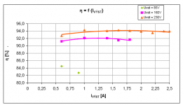
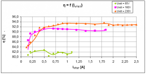
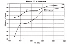
No, there are no measurement errors. But it was hitting 94,3% at about 300W output, at 1kW it was 94,0 (see figures). But it must be said that we did measure the input power BEFORE the mains rectifier, so the rectifier losses are counted in the overall efficnency. The rectifier power loss at full power was, by simulation, about 20W at 350Vac. If we would measure the input power AFTER the rectifier, the efficiency would be higher by about 2% which is in good agreement with the measurement made by Texas Instruments in UC3855 app. note (slua146a) where they measured the DC input power and got about 96% efficiency with similar measurement conditions (see figure - "Conventional").
So how are you measuring the input power? Are the rectifier losses accompanied in your efficiency calculations?
Attachments
Last edited:
- Status
- This old topic is closed. If you want to reopen this topic, contact a moderator using the "Report Post" button.
- Home
- Amplifiers
- Power Supplies
- 1kW PFC-Boost