Hello,
Thanks Black Heart and other for sharing your experiences.
In a previous post the option of CCS was mentioned.
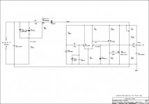
I’ve added the schematics of the shuntreg of Manfred Huber. Kind enough it was freely available on his site for a long time. It is a version to supply power to a tubed preamp.
The CCS is supposed to isolate the power supply from influences of the the mains and many reported elsewhere that it does so indeed. In words of Manfred Huber: ‘Using a current source to supply the shunt reg helps even more as the high impedance of the CS shields the B+ line from the power transformer and the rectifier.’
Here’s also the quote of Hubers explanation on the part of how the CCS works:
‘C1 is here to provide a low impedance to the current source at high frequencies. This helps to prevent the CS from getting unstable. Note that in a real circuit C1 is in parallel with the filter cap. C1 may be omitted if the interconnection from the filter cap to the CS is short.
D2 is an integrated shunt voltage regulator that works like this: It measures the voltage from its cathode (8) to the reference input (5) and tries to keep this voltage constant at 1.223V. It does this by draining more current from cathode (8) to anode (4) as the control voltage rises. If we try to draw more current from the CS the voltage over P1 and R2 rises and D2 drains more current. Next the voltage on the anode of D2 (4) rises and the gate-source voltage of Q2 drops. The impedance of Q2 rises and the current supplied by the CS drops. The feedback loop is closed.
Q1 and R1 form a current source that supplies the bias current needed by D2. Note that Q1 is a depletion-mode mosfet. This means it draws current when its gate source voltage is zero. If you know the supply voltage at which you want to use the CS you can substitute a simple resistor for Q1 and R1 that is calculated to sink about 1mA of current at the actual operating voltage.
If for some reason the CS sees no load it will saturate and D2 will stop draining current. The anode voltage would drop to ground level while the cathode would remain at B+ potential. This means that suddenly D2 would see the whole supply voltage. If this happened D2 would die immediately! The Zener diode D1 was included in the circuit to avoid this problem.
R3 prevents HF oscillations of Q2. D3 was included to avoid reverse current through Q2 during power down.’(end of quote).
The CCS-principle in the Huberdesign might be valid for the low voltage design in this thread. Note the use of a depletion mosfet, but with an extra voltage also a ‘normal’ mosfet might be usable (I think, with my modest EE-knowledge).
Would anyone care to comment on what change has to be made to make this possible in practice?
Best regards, Arjen.
Thanks Black Heart and other for sharing your experiences.
In a previous post the option of CCS was mentioned.
I’ve added the schematics of the shuntreg of Manfred Huber. Kind enough it was freely available on his site for a long time. It is a version to supply power to a tubed preamp.
The CCS is supposed to isolate the power supply from influences of the the mains and many reported elsewhere that it does so indeed. In words of Manfred Huber: ‘Using a current source to supply the shunt reg helps even more as the high impedance of the CS shields the B+ line from the power transformer and the rectifier.’
Here’s also the quote of Hubers explanation on the part of how the CCS works:
‘C1 is here to provide a low impedance to the current source at high frequencies. This helps to prevent the CS from getting unstable. Note that in a real circuit C1 is in parallel with the filter cap. C1 may be omitted if the interconnection from the filter cap to the CS is short.
D2 is an integrated shunt voltage regulator that works like this: It measures the voltage from its cathode (8) to the reference input (5) and tries to keep this voltage constant at 1.223V. It does this by draining more current from cathode (8) to anode (4) as the control voltage rises. If we try to draw more current from the CS the voltage over P1 and R2 rises and D2 drains more current. Next the voltage on the anode of D2 (4) rises and the gate-source voltage of Q2 drops. The impedance of Q2 rises and the current supplied by the CS drops. The feedback loop is closed.
Q1 and R1 form a current source that supplies the bias current needed by D2. Note that Q1 is a depletion-mode mosfet. This means it draws current when its gate source voltage is zero. If you know the supply voltage at which you want to use the CS you can substitute a simple resistor for Q1 and R1 that is calculated to sink about 1mA of current at the actual operating voltage.
If for some reason the CS sees no load it will saturate and D2 will stop draining current. The anode voltage would drop to ground level while the cathode would remain at B+ potential. This means that suddenly D2 would see the whole supply voltage. If this happened D2 would die immediately! The Zener diode D1 was included in the circuit to avoid this problem.
R3 prevents HF oscillations of Q2. D3 was included to avoid reverse current through Q2 during power down.’(end of quote).
The CCS-principle in the Huberdesign might be valid for the low voltage design in this thread. Note the use of a depletion mosfet, but with an extra voltage also a ‘normal’ mosfet might be usable (I think, with my modest EE-knowledge).
Would anyone care to comment on what change has to be made to make this possible in practice?
Best regards, Arjen.
Attachments
Just one quick point about the "traditional" shunt regulator schematic I posted in http://www.diyaudio.com/forums/showthread.php?postid=712031#post712031, Walt Jung was kind enough to point out to me that having a CM voltage of 3.2 is close to the edge with the old fet opamp types like the AD711 series. It is usually spec'd as around 3.5V above V-, and could go as much as 4.0 at temp extremes, meaning that it would be better to use a more conventional reference with a higher voltage in a regulator with the opamp V- connected to ground. The first schematic I posted of my actual DAC regulator is OK since I use +/- 5V supplies on the opamps and so the CM voltage is not a problem. I have used regulators with both a lithium cell reference and the opamp V- connected to ground without any problems. In fact, in that same DAC I pulled the first schematic from, I also use the regulator shown below for the isolated PLL power (also using the same type of L-C filtering as the others) with no problems for the last few years, but just wanted to pass it on that it could lead to a potentially serious phase reversal problem under certain conditions. Thanks Walt!
An externally hosted image should be here but it was not working when we last tested it.
ccs and shuntreg
Hello,
To set a ccs and shuntreg combination at the right current I notice in various publications the opinions differ some.
The advantage of a ccs is that it isolates the load from any variations in mains/secundairy voltage. The ccs must provide current for the total sum of currents for the shuntreg and the load. In such a design it comes in handy when the load has a near to stable current demand, like class A designs.
The shuntreg itself needs current to have enough stabilising power and it must be able to absorb any variations in current of the load.
Some say the shunt reg should be set at a minimum of 10% of the load current. I wonder if this is inclusive of exclusive of the power consumption of the shuntreg itself. Other go as far as stating that the shuntreg must be set at the same current as the load in order to work properly.
This brings me to the question what are the proper design issues for a ccs in combination with the shuntreg of Black Heart?
Any suggestions?
I wonder if anyone with EE-background already had time to take a look at my question in post #21?
Best regards, Arjen.
The pic you have attached, I beleive, doesn't match the circuit description you've provided.
The simple answers to your Qs:
1. The ccs must provide current for the total sum of currents for the shuntreg and the load.
2. The shuntreg itself needs current to have enough stabilising power and it must be able to absorb any variations in current of the load.
So, if you know your load current variation (let's say, for example, from 20 mA to 160 mA), you can choose the shunting element minimum current to assure its proper operation at that minimum current (no oscillation, low enough dynamic impedance...), lets say, at 13 mA.
Now, your CCS is supposed to be set at 13+160=173 mA (with the ability to dissipate the power it is consuming).
When the load will be consuming that minimal level of 20 mA,173-20=153 mA will flow through the shunting element/block, so, the shunt suppose to be able to absorb that current without excessive heating, and with no oscillation.
ccs and shuntreg
Hello StevenOH, others,
Thanks for your kind and clear reply.
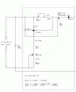
Yes, the picture I added in post #21 didn’t match the text.
The picture is a simplified version of the original. I’m sorry for this mixing up. I’ve added the CCS-part of the original with this post. Comparison of the two CCS-versions is mainly: As you can see from the original the LM4041 was replaced by an LM329 (together with D1 by C2) and the lower CCS was repleced by a simple resistor R1.
The function of both CCS-es is the same.
I think components for the simple version might be more easy to source (like at Farnell in One). To calculate the CCS-current I found in my notes on the simple version of post 21 the following formula: current is about I = 3V / R2.
I’ve also found a CCS-shuntreg version of Emile Sprenger that uses a ‘normal’ mosfet instead of a depletion one. This design was also meant for a tubed power supply. I’ll post the CCS-part of it in a next post.
When I understand it right one could calculate the neede current for the load first. Or simply measure its needs and variation first real life by using a conventional power supply. Also the current of the applied shuntreg can be calculated, like the one of Black Heart.
Then one could apply your guidelines, SteveOH, to set the current with the right margin.
In order to do that properly one could add a 10 ohm resistor in series with the power transistor/mosfet of the shunreg and a 10 ohm resistor in series with the load. With two voltage meters one could easily follow upon installation how the currents behave.
The only question that rests is the following. The CCS-part of Huber was designed for a high voltage power supply of a tuber preamplifier and the parts are specified for it. Can this CCS be used for low voltages? Of course the voltage requirements are lower then, so more freedom of parts choice and smaller dimensions. Also the power dissipation will be lower for the active components. But is that all there is to it?
Can anyone comment on this?
Best regards, Arjen.
Hello StevenOH, others,
Thanks for your kind and clear reply.
Yes, the picture I added in post #21 didn’t match the text.
The picture is a simplified version of the original. I’m sorry for this mixing up. I’ve added the CCS-part of the original with this post. Comparison of the two CCS-versions is mainly: As you can see from the original the LM4041 was replaced by an LM329 (together with D1 by C2) and the lower CCS was repleced by a simple resistor R1.
The function of both CCS-es is the same.
I think components for the simple version might be more easy to source (like at Farnell in One). To calculate the CCS-current I found in my notes on the simple version of post 21 the following formula: current is about I = 3V / R2.
I’ve also found a CCS-shuntreg version of Emile Sprenger that uses a ‘normal’ mosfet instead of a depletion one. This design was also meant for a tubed power supply. I’ll post the CCS-part of it in a next post.
When I understand it right one could calculate the neede current for the load first. Or simply measure its needs and variation first real life by using a conventional power supply. Also the current of the applied shuntreg can be calculated, like the one of Black Heart.
Then one could apply your guidelines, SteveOH, to set the current with the right margin.
In order to do that properly one could add a 10 ohm resistor in series with the power transistor/mosfet of the shunreg and a 10 ohm resistor in series with the load. With two voltage meters one could easily follow upon installation how the currents behave.
The only question that rests is the following. The CCS-part of Huber was designed for a high voltage power supply of a tuber preamplifier and the parts are specified for it. Can this CCS be used for low voltages? Of course the voltage requirements are lower then, so more freedom of parts choice and smaller dimensions. Also the power dissipation will be lower for the active components. But is that all there is to it?
Can anyone comment on this?
Best regards, Arjen.
Attachments
<<Can this CCS be used for low voltages? ... is that all there is to it?>>
Two main requirements for CCS are:
1. High dynamic impedance at the specified voltage drop (across it) and currents range.
2. Low and, possibly, stable internal capacitances to maintain that high impedance into the high frequencies of interest and to avoid parasitic oscillation.
P- type devices usually have worse characteristics than N- type: their drain/collector dynamic impedance typically is less and drops with lower voltage, and capacitances are higher. In addition, with lower voltage across any transistor (less than ~10 V) these capacitances are rapidly increasing in nonlinear fashion.
The simple test for your CCS suitability is to supply it from it's intended voltage supply THROUGH variable resistor (to model the load) and current meter, and to measure the voltage drop on CCS with variable current. It would be good, if you were able to do impedance measurement on high freq too. You can monitor CCS propensity for oscillation with any known tricks (TV set, AM/SW/FM radio) for noncontact pickup.
If you will need to improve your CCS for the lower voltage application, N-channel Ench. (or Depl.) Mosfet with lower max. specified voltage, capacitances (especially, Crss, Coss) and Rds(on) will be the next choice.
Hello StevenOH,
Thanks; I learn that you encourage to just try the CCS and measure what's happening. Ok, it might take some time (like in automn) and it's worth it. When ready I'll report. Or anybody else that feels invited to do so.
Don't know if I manage to measure impedance though.
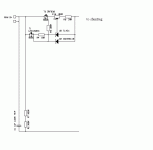
For your information I've added the CCS-part of the design of Emile Sprenger as said in my previous mail.
Best regards, Arjen.
Thanks; I learn that you encourage to just try the CCS and measure what's happening. Ok, it might take some time (like in automn) and it's worth it. When ready I'll report. Or anybody else that feels invited to do so.
Don't know if I manage to measure impedance though.
For your information I've added the CCS-part of the design of Emile Sprenger as said in my previous mail.
Best regards, Arjen.
Attachments
")
Black Heart said:
Thanks Black Heart for those kind explanation---BUT...
What's wrong with links on post 9 and 10 from?
here's an article by Ron Mancini from Texas Instruments which appeared in EDN last winter -- how to make a good reference into a great reference:
EDN PDF
Very interesting article, thanks for posting.
MAX6126 is clearly a bandgap reference
(From maxim-ic.com)
SUNNYVALE, CA-November 13, 2002-Maxim Integrated Products (NASDAQ: MXIM) introduces the MAX6126, the industry's lowest noise, ultra-precision bandgap voltage reference.
INDUSTRY'S LOWEST NOISE, ULTRA-PRECISION, VOLTAGE REFERENCE IDEAL FOR HIGH-RESOLUTION DACs - New Product Release
Nationals own best reference LM329 is a buried Zener reference, which according to the article above has much lower basic noise. A reading of datasheets show a difference of something like 3 times more noise in MAX6126 compared to LM329. The article says 6 - 30 times difference.
Did anyone make a direct comparison of these two voltage references?
unfortunately not upload here - only under http_members.mailaka.net/davey/reg.gifAnd here's a more traditional shunt regulator approach, while still keeping the lithium battery as a reference ... the feedback resistor value depends on the output voltage you want to get 3.2V at the -input, and the series resistors depend on the current. The only thing fixed in this design is the use of the AD711 series for the opamp. There are a few other types that can be used but most opamps input circuits will discharge the battery when powered off so if you don't use the AD711 you'll need to test it with a high value resistor in series with the battery to measure if there is any leakage current into the opamp. It should be zero. Some other types might also have trouble with the reference at the same level as the + supply, as it is on the tracking negative regulator.
An externally hosted image should be here but it was not working when we last tested it.
even on webarchive not saved. Maybe a member can upload the file here.
I want also to know more, if there are such a paper - thank you.Jan Didden:
Was there an article associated with the pdf schematic that you attached in post #2? If there is, I'd be interested in reading it.
regards, jonathan carr
My own topology is a discrete CCS version - go to post #8 under
http://www.diyaudio.com/forums/anal...ences-between-mark-levinsons-jc-1-jc-1dc.html
(first pdf)
Last edited:
- Status
- This old topic is closed. If you want to reopen this topic, contact a moderator using the "Report Post" button.
- Home
- Amplifiers
- Power Supplies
- Shunt-regulated 24V DC Power Supply for Preamp Modules